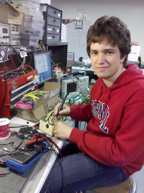
Introduction
Our project records and extracts event-related features from a 36-point relative blood-oxygen concentration sensor array from the surface of the brain.
We chose this project because of a combined interest in brain-computer interfaces. In an attempt to balance cost, complexity, and sensor density, we decided to implement a NIRS-inspired system. After collecting data from the array, the results were sent to a computer and displayed in a Java GUI.
High Level Design
Rationale and Sources
Several popular methods of measuring brain activity are electroencephalography (EEG), magnetic resonance imaging (MRI), positron emission topography (PET), computed axial tomography (CAT), magnetoencephalography, and near-infrared spectroscopy (NIRS). Of these methods, only EEG and NIRS are within any measure of feasibility given our time and budget for this project. MRI uses a powerful magnetic field, PET uses radiations from a nuclear tracer, CAT uses X-rays, and MEG uses unobtainable superconducting magnetometers. EEG is based on picking up electric fields resulting from the electric pulses of the underlying neurons. NIRS, on the other hand, works by shining infrared light into the scalp and measuring the amount of reflected light with a series of phototransistors. Since blood reflects infrared light depending on its level of oxygen concentration and activity within a region of the brain corresponds to increased blood flow to that area, the reflected infrared lights is a measure of local brain activity. The EEG is able provide a lot of information with high temporal resolution at the price of less-trivial sensor implementation than NIRS. Without amplification potentials measured at the scalp are on the order of microvolts whereas initial NIRS signals can be as high as the 10 mV range. Since we want high sensor density, the lower cost and easier implementation of an NIRS system are very desirable.
We used Shirley M Coyle’s 2007 paper on a brain-computer interface using NIRS to help provide a proof of concept and reference for our system. Initially we prototyped with phototransistors/LEDs that are slightly beyond the upper window for NIRS (940nm vs 900nm), but we continued to use the 940nm pair after seeing data very similar to that in Coyle’s work.
Normally, the goal of NIRS (when applied to a human subject) is to produce an absolute measure of oxygen concentration. Since blood has different absorption curves for infrared and red light (as shown to the right), the ratio of reflected red and infrared light can be used along with said curves to yield an absolute concentration. However, since we are only interested in the relative change in blood oxygen concentration, a single infrared light source is sufficient.
Logical Structure
The system is broken into five stages: sensor array, filter/amplify, ADC, on-chip processing, and reporting.
Hardware Structure
The 36 sensors are arranged in a 2-by-18 grid on a flexible wire mesh. Each sensor consists of a single infrared LED and phototransistor. The array is able to conform to an individual’s head with minimal effort. The wires connecting the array to the rest of the system effectively hold the array at approximately head-height due to their memory. To bring the array in closer contact with the head, a wire is pulled from both sides of the head. Once the array has reached an acceptable location, the wire can be twisted and the array will remain in its current location.
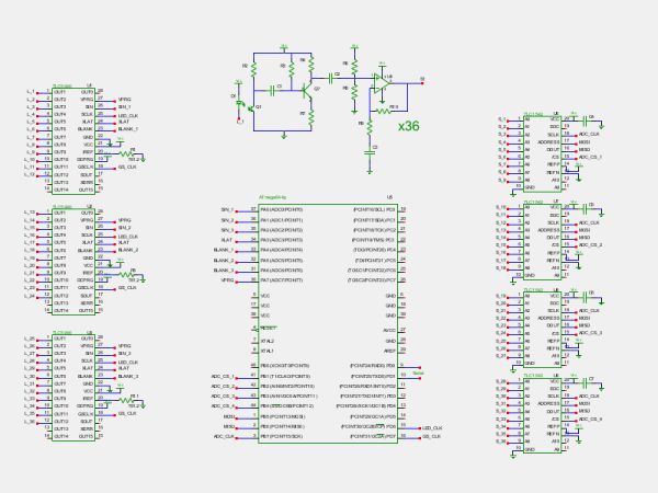
Since the signal from the phototransistor is 10-20mV peak-to-peak with a DC bias of about 4V, it is sent to a filter/amplifier boards. These boards consist of a common-emitter pre-amplifier, re-biasing stage (to 2.5V) and an active non-inverting AC amplifier. This allowed the system to have a much larger dynamic range without sacrificing the low-frequency information we are interested in. The signal is then sampled by an ADC and sent to the microcontroller over SPI. The microcontroller can selectively turn a sensor’s LED on or off so that adjacent sensors do not interfere with each other.
Software Structure
The microcontroller simultaneously samples from each of 36 sensors, processes the data, and transmits the results to a laptop running a Java GUI for display.
The sensor array was arranged so that multiple phototransistors would be able to receive light from multiple LEDs. However, in an attempt to minimize the non-ideal variations between sensors, the microcontroller turns on LEDs such that a phototransistor is only activated by its own LED (however, the user can selectively turn off sensors from the Java GUI). Consequently, this means that the microcontroller skips over ADC channels if they correspond to a sensor that has its LED turned off. After sampling, the results are displayed in a Java GUI in three ways: a plot of raw time-domain data, a false-color representation of average relative oxygen concentration, and a likelihood graph of possible trends in the data.
Hardware/Software Tradeoffs
Much of the analysis between a hardware and software tradeoff was done during construction of the system. Even though we had a large amount of time between samples (about 18 ms) we wanted a the software system to be as efficient as possible in anticipation of extra signal processing. Shortly into our physical build, however, we made the decision to trade code efficiency with lower soldering difficulty/time.
One example of such a tradeoff was with the inputs to the ADC chips. Initially three of the ADCs would receive 11 of their sensor grouping (0, 1, or 2, as discussed below in hardware design). The fourth ADC would only then need to take in three inputs, one from each sensor group. This approach had rather simple software behind it since the microcontroller read from ever ADC port of the first three ADCs. After physically arranging the ADC and amplifier boards, it became apparent that the uneven distribution of ADC inputs would create a dense region of wires. To avoid this, the inputs were balanced and each ADC took in nine inputs. The resulting product had a more uniform distribution of wires.
Standards
Our system has no relevant interface standards. We specified our own custom serial packet for efficient communication between the microcontroller and the Java GUI.
Intellectual Property
We were unable to find many patents relevant to our project. One patent we did find was US 2011/0105909 A1. It describes a form of a brain-computer control interface using near-infrared light to measure eye response to different images. This is sufficiently different from our project.
Hardware Design
Our project has three large hardware components: the sensor array, the amplifier boards, and the shoulder-mounting unit.
Sensor Array
Electrical
The sensor array consists of 36 pairs of infrared LEDs and phototransistors. The LEDs are powered by the LED driver chips located just behind the array. The drivers provide a constant current sink for all channels with the maximum current set by a single resistor (per chip). The formula is the following
where Vref is 1.24 V. Each LED driver also has the ability to adjust the current flowing into each port independently through a method called dot correction. The chip provides 64 steps of the current ranging from 0% to 100% of the maximum current as specified by the above equation. Dot correction allows the system to selectively turn a given sensor’s LED on or off. All LEDs of a particular LED driver could be turned off at once by pulling the BLANK pin low. This method was used to quickly prepare the array for sampling. The LED drivers are actually meant to drive the LEDs with a PWM, but this was not desired for this system. To trick the chip into keeping the LEDs on, the PWM period values were written to their maximum and the PWM input to the chip was pulsed once after initially writing to the LED driver. This way, the LED driver would turn on the desired LEDs and keep them on until the microcontroller sent a command telling it otherwise (through either the BLANK pin or reprogramming the dot correction values).
For more detail: BrainMap: fNIR imaging of the brain Using Atmega644