Introduction
The CCDImager is an Atmel Mega32 microcontroller driven imaging system that uses a Charge-Coupled Device (CCD) optical sensor to capture a still image.
The purpose of this project was to design a basic imaging device from first principles. While brainstorming for ideas for the final project, we came across several varied applications of microcontrollers, from music synthesis and processing to wireless communication. Going through several previously implemented ideas, we noticed that the use of the Atmel Mega32 microcontroller for imaging had not yet been attempted. After further research, we realized that fast, inexpensive and digitized imaging using the Mega32 is possibly among the harder, and hence more interesting applications of microcontrollers. This turned out particlarly true given the processing speed limitations of the Mega32, the budget constraints of this project, and performance limitations of common analog hardware parts at high frequencies. To be able to contend with these limitations and develop a reasonable product, our goal was to gain as much exposure to hardware design concepts as possible, as well as utilize the AVR architecture, C and assembly language abilities we had developed in this course.
High Level Design
The source of inspiration for our project was a dirty old Epson scanner that we stumbled upon in our dorm. Since any scrap parts we gathered were not counted in our budget, we had been collecting any and everything that could possibly have been of use. While thinking about final project ideas, we decided to take apart the scanner, and research into how it works. The online literature indicated that several scanners use CCD image sensors, and further reading sparked an interest in CCD sensors.
After a detailed search, we decided to use Texas Instrument’s TC237B CCD Image Sensor, since it has good resolution (680×500 pixels), scope for anti-blooming, high sensitivity, and NTSC compatibility, which would ease adaptation to video applications. The TC237B has an internal structure that converts the charge stored in its charge wells due to incident light, into voltage at 12µV per electron. This voltage is transferred out from the CCD by sending it a series of pulses for row and column transfer. These will be described in detail later.
In order to be able to process the CCD’s outcoming voltage signal, a high speed digitizer was necessary. This digitizer, often referred to as the “analog front end,” acts as a fast ADC, with an inbuilt structure that is particularly useful for digitizing CCD voltage waveforms. The Analog Devices AD9822 seemed like a good choice because it has a 14bit, 15MSPS ADC, and is specific to CCD applications.
The Atmel Mega32 has an onboard 2KB RAM. However, for digitizing the 340,000 pixels of the CCD sensor at 2 bytes/pixel, this was highly insufficient. As a result, we decided to use an external SRAM to store the digitized output of the AD9822, and then transfer it into the Mega32 from this internal memory. We chose Cypress Semiconductor Corporation’s CY7C1048CV33, a 4MB (512 x 8) Static RAM chip, because of its ease of control due to TTL-compatible inputs and outputs, low power usage, high speed, and its generous storage capacity.
Hardware Design
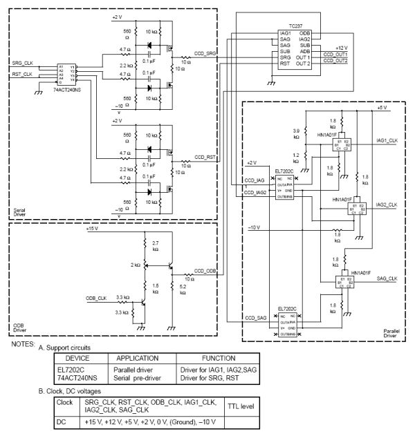
The first concern in hardware design was the design of a circuit to provide the necessary voltage signals and swings to the CCD sensor. As a first approach, we studied the datasheet of the TC237B CCD sensor in order to see what circuit would fulfill the necessary specifications. However, the “Recommended Operating Conditions” specified by the datasheet required voltage levels up to 26V. This was beyond what the voltage supplies available in lab could provide. As a consequence, we tried looking into making our own voltage supply circuits using voltage regulator chips and a 30V power supply we were able to borrow. However, this proved to be a rather daunting task as we required at least seven different voltage levels for the CCD to operate properly, and this would have meant that a lot of hardware resources (solder boards and so forth) would have been taken up by just the voltage supply circuits. In addition, the couple of test circuits we attempted did not hold very regular voltage levels. After seeing these disappointing results, we decided to look at the online literature for information on alternate implementations of the CCD voltage levels. There seemed to be major differences in the various literature we studied. In the end, we decided to implement the circuit provided by Texas Instruments in the CCD datasheet under “Application Information,” even though the voltage levels suggested in that circuit did not agree with their own “Recommended Operating Conditions.” This circuit is shown and explained below.
The CCD sensor requires the following signals: CCD_ADB, CCD_SRG, CCD_RST, CCD_ODB, CCD_IAG1, CCD_IAG2, and CCD_SAG. The CCD_ODB provides an overflow drain bias for anti-blooming the charge wells so that there is less smear between neighboring pixels. An application of a minimum 1µs pulse on this signal sets the clearing and integration phase in which charge is collected on the charge wells. The CCD_IAG1 and CCD_IAG2 signals provide the voltage to drive the image gate areas 1 and 2 respectively. In progressive-scan timing with single register readout (the mode we implemented), the CCD_IAG1 and CCD_IAG2 signals are tied together. The CCD_IAG signals, along with the CCD_SAG (for the storage area gate), drive the collection of charge in the charge wells and its parallel transfer from the image area to the storage area. The CCD_SRG signal then begins the serial transfer of the charge out from the storage area, onto the output pins CCD_OUT1 and CCD_OUT2. The CCD_RST then resets the gates during serial readout. The CCD_ADB signal is the supply voltage for the amplifier drain bias. This means that the CCD is effectively on when this voltage is supplied. As a result, this signal is at its high value during the course of the above mentioned steps of exposure, integration, parallel transfer to the storage area and serial transfer out of the storage area. The MAX333A single-pole double-throw (one control line for two selectable lines – three way switch) was used to switch the CCD_ADB signal on and off since it is very fast and can handle large voltage swings. The CCD datasheet recommended a frequency of 12.5MHz to drive the CCD_SRG, CCD_RST, CCD_IAG1, CCD_IAG2, and CCD_SAG signals. However, our tests for the crystal oscillator circuits for the 12.5MHz and 5MHz showed that the 12.5MHz signals were much more noisy than the 5MHz signals, so we tried using a 5MHz frequency for these signals. This succeeded in driving the circuit, so we made a design change from 12.5MHz to 5MHz for these signals. The crystal oscillator circuit is described later. All voltage signals to the CCD are in reference to the CCD_SUB (substrate) voltage, which is connected to ground in this implementation.
The circuit in Figure 2 is thus divided into three main parts: (1) Serial Driver, (2) ODB Driver, and (3) Parallel Driver.
(1) Serial Driver Circuit
In our execution of the serial driver circuit, we implemented the PMOSFET switches with the npn TIP31 transistors, and the NMOSFET switches with the pnp TIP32 transistors. For the diodes in the figure, 1N914 diodes were used. The generation of the SRG_CLK and RST_CLK signals is described in the Interface Design section. Once these signals are obtained by the serial driver circuit, they are put through a tri-state octal buffer (74ACT240NS), which inverts the incoming SRG_CLK and RST_CLK signals, and also helps restore the incoming signals to TTL logic levels if they were attenuated by noise. The alternate high-low nature of the signals coming out of the 74ACT240NS buffer alternate which transistor (TIP31 or TIP32) is on, and therefore switches between the 2V and -10V supplies.
(2) ODB Driver Circuit
The npn transistors in the ODB driver circuit were implemented using 2N3904 npn transistors. When a TTL logic high signal is sen on the ODB_CLK line, the 15V supply is selected by the pair of npn transistors. When the ODB_CLK line carries a logic low, CCD_ODB switches to the ground-level voltage of 0V. The ODB_CLK signal is generated by the microcontroller. This is described in the Interface Design section.
(3) Parallel Driver Circuit
The Toshiba HN1A01F dual epitaxial general purpose transistor chips are no longer produced, so we used an equivalent chip, the IMT1AT110. Again, the generation of the IAG1_CLK, IAG2_CLK and SAG_CLK are described in the Interface Design section. Close inspection of this circuit reveals that since the emmiters of the transistors are shorted and taken to 5V supply through a resistor, there is a voltage divider between the 5V supply anf one of the bases, and the collector on one side is taken to the low voltage of -10V, the construction is that of a current mirror. This is to make an ad-hoc scheme for amplification of the incoming signal. Transistors can switch at frequencies up to 100MHz, and this provides a convenient way of achieving amplification that would have been impossible to implement with other relatively slow amplification methods such as using op-amps. This amplified signal is then fed into the EL7202C non-inverting high-speed power MOSFET driver. This chip regulates the relative phases of the CCD_IAG and CCD_SAG waveforms so that they are fed to the CCD one cycle out of phase.
The memory and CCD digitizer circuits were constructed according to their datasheets and as described in the Interface Design section. Again, we found that the lesser noise carrying 5MHz frequency worked with the CCD digitizer, so we made a design change to switch from 12.5MHz to 5MHz.
Parts List:
| Part | Quantity | Total Price | Notes |
| TC237B CCD Image Sensor | 1 | $0.00 | Sampled from Avnet |
| ATMega32 | 1 | $0.00 | Sampled from Avnet |
| CY7C1049CV33 SRAM | 1 | $0.00 | Sampled Cypress Semiconductor Corporation |
| AD9822 | 1 | $6.94 | Digikey |
| Solder boards | 3 | $7.50 | |
| Custom PC board | 1 | $5.00 | |
| RS232 Connector | 1 | $1.00 | |
| Power Supplies | 3 | $15 | |
| MAX233 | 1 | $0.00 | Sampled from Maxim IC |
| MAX333A | 1 | $0.00 | Sampled from Maxim IC |
| IMT1AT110 | 3 | $1.44 | Digikey |
| SN74ACT240NS | 1 | $0.56 | Digikey |
| SN74LS00 | 2 | $0.00 | From Lab |
| SN74LS240 | $0.00 | From Lab | |
| SN74LS241 | 2 | $0.00 | From Lab |
| EL7202C | 2 | $0.00 | Sampled from Intersil |
| TIP31 | 2 | $0.00 | From Lab |
| TIP32 | 2 | $0.00 | From Lab |
| 1N914 | 4 | $0.00 | From Lab |
| Crystal Oscillators | 5 | $3.56 | |
| Capacitors, Resistors, Pots | $0.00 | From Lab | |
| TOTAL COST | $41.00 |
For more detail: CCD imager Using Atmel Mega32