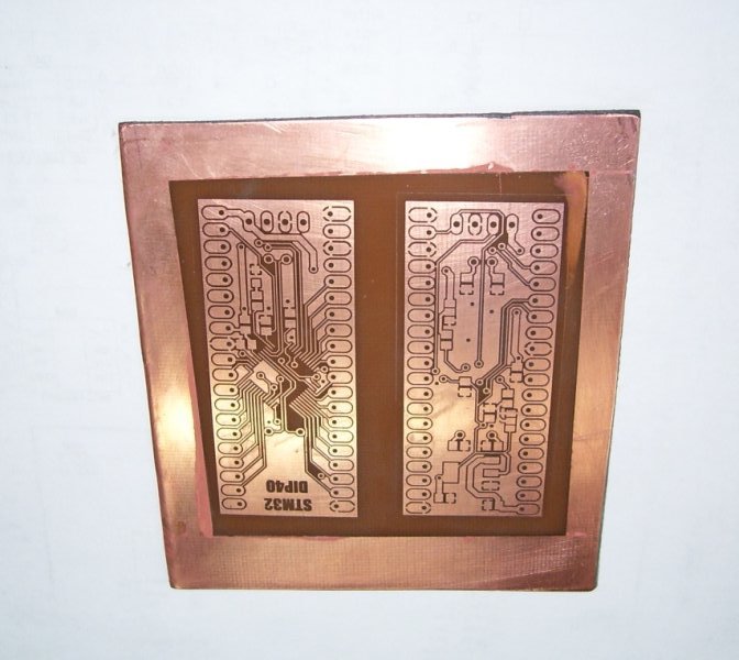
Catching up the development of printed circuit boards at home i often faced with the problem of “the bulbous” vias. Usually homemade double-layer boards soldering from both sides with the thin wire, the result usually satisfied but if you need to make VIA under the chip TQFP48, SOIC16 and that’s is a real problem, if contact is very bulbous it will be simply impossible cleanly solder chip as its legs will hang in the air.
I suggest you create your own version of flat vias.
Creating quality board begins with the development of high-quality template for illumination Resist. I created the PCB in program EAGLE it is very comfortable and in internet is enough libraries elements and examples of use.
1.I cut out board with a offset of 15 mm on each side bigger than the resulting board.
2.Before application of Resist carefully grind with a sandpaper (especially the edges of burrs) wash with powder detergent such as “Gala” and sponge
For more detail: DIY PCB with flat VIA’s

