Contents
hide
Introduction
Short Summary
This project allows a Wonderswan developer to upload 64 kB of code/data and execute it on real Wonderswan handheld gaming hardware.
Long Summary
-
- We started by opening up one of our Wonderswan cartridges and identifying the various chips and circuitry found inside. We found the main ROM chip, and guessed that it would follow standard JEDEC pinouts for programmable ROM chips of this nature. Having a nonstandard pinout would’ve increased production costs. We then mapped the pins on the cartridge edge connector to the pins on the ROM chip, so we had a rough idea of what type of chip it was and how the address and data lines were connected.
- After verifying possibility of success, we proceeded to build a memory programmer. Since the Wonderswan uses a 16bit wide word data bus, we purchased two SRAM chips, each 8bit wide. We then chained these together to provide a total of 32768 16bit words over a 15bit address space. Since the Wonderswan and our MCU operated on different voltages and we didn’t have enough pins on the MCU to directly address all 31 lines and still be able to communicate over a serial line, we built a demultiplexer circuit out of 74AHC logic family chips. This allowed us to buffer out the various lines over time, and also allowed us to drive a 3.3V output level chip with 5V signals.
- After the hardware was built, we programmed on the MCU a XModemCRC compatible transfer program so that we can both upload and download from our “cartridge.”
- In order to interface with the Wonderswan, we etched our own board using a laser toner transfer method, and trimmed it so that it fit into the cartridge slot on the Wonderswan. After everything was attached, we realized that the Wonderswan had a hardware handshake to check for valid cartridges. A valid cartridge has a custom chip, which we could not reproduce. Thus, we tricked the Wonderswan into accepting our cartridge by booting into its preferences mode (which needs a cartridge to load up but doesn’t run off the cartridge), and then inserting our cartridge and letting the mode continue to normal play.
High Level Design
Origination of Idea
-
- The Wonderswan was a handheld console that gained a decent amount of popularity, but eventually died because the GameBoy Advance came out with a plethora more games, backed by video game superpower Nintendo. The Wonderswan used a popular architecture, the x86, for its processor and thus there were many tools available to compile compatible code. Eventually, Qute corporation released a development kit it called the WOnderwitch, which allowed users to create their own Wonderswan games. The problem with using something like this was that program size was severely limited to around 64kB, and one had to use the built in software interrupt driven functions for interacting with the hardware. This limited the versatility of this device. Furthermore, the Wonderwitch went out of production along with the Wonderswan, and current fetching price is around $150-$200, which is approximately 2-3 times the cost of a new Wonderswan.
- In order to further development in this area, we decided that it would be a neat idea to reverse engineer how a Wonderswan cartridge would work, and build our very own cartridge with which to upload and test programs with. The API for the Wonderswan has been mostly reverse engineered, but there are still quirks that are unknown. Hopefully, by creating a programmable cartridge and by publishing the specs for the cartridge format online, we can encourage further development on this dying console.
Logical Structure
-
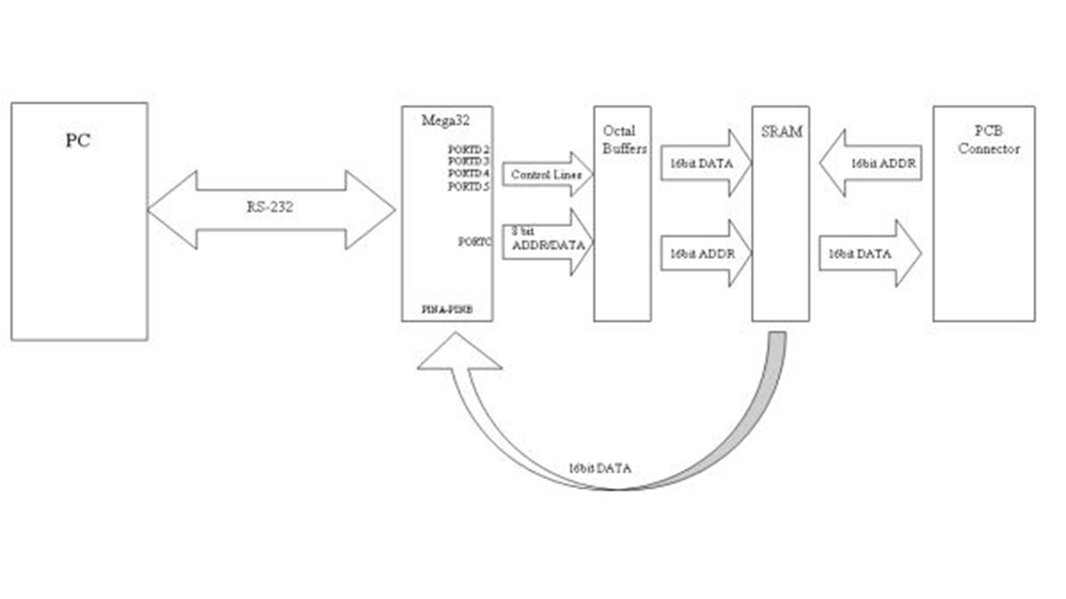
- The program on the MCU essentially controls the programming of the 2 SRAM chips in our circuit. Its output is sent through 4 octal buffers so that we can get a 3.3V signal going to the SRAM. It also has control signals which allow it to separate the buffers and itself from the SRAM when it’s not using it. This allows the Wonderswan to interoperate with the circuit even with the MCU running.
- The hardware is essentially in three pieces. One piece is the set of buffers which act as a demultiplexer for the limited number of pins the MCU has. It also doubles as a level converter to output 3.3V instead of 5V. The second piece is the set of SRAM chips. These do the actual storage of program information for the Wonderswan. The last piece is the cartridge PCB, which is essentially a connector to allow the SRAM to connect to the Wonderswan hardware.
Hardware/Software Tradeoffs
-
- The MCU wasn’t fast enough to fetch instructions for the Wonderswan in real time, because the Wonderswan can fetch at a maximum rate of two bytes per 3.072 MHz clock tick. Furthermore, the MCU did not have enough storage to even hold one bank (64kB) of Wonderswan programming. Thus, we decided to delegate this functionality to a set of SRAM chips, which are faster (120 ns speed, which is like 2 cycles on the MCU).
- Instead of having control signals feeding straight into the buffers and SRAM, we decided to use hardware inverters. The inverters are tied to a default state if the MCU is not on, so that we do not keep certain inputs floating. Furthermore, these default states represent a “safe” state for the buffers, so in these states the buffers have their output turned off and the SRAM is in read mode. Lastly, an input of 0 to these inverters generate the safe state, so the MCU can boot up and accidentally send a 0 to all the control signals and still remain a safe state.
Relevant Standards
-
- XModem CRC
We implemented a scaled down version of XModem CRC to the point that we could transfer data back and forth between the computer running HyperTerm and the MCU. - JEDEC Standard No. 21-C
The MASKROM on one of the Wonderswan cartridges looked like it would follow the JEDEC word-wide EPROM standard for pinouts. We’ve verified at least the lower 15 bits of address, the data bits and the output enable lines to be correct.
- XModem CRC
Intellectual Property Considerations
- As for intellectual property, it may seem at first that we are violating the DMCA. First, we are not sure that obscurity of hardware specifications is an actual protection and we do not know of any actual protection schemes in use. The valid cartridge detection scheme does not seem to be a protection mechanism and only seems to be a validation mechanism to insure that connections to the cartridge are correct. Furthermore, we are not creating a device to bypass this, since the functionality is already in the Wonderswan to bypass it. We only discovered this functionality and thus did not create it.
- A recent exemption has also been added to the DMCA by the Library of Congress on October 28, 2003. It states that there’s an exemption for
“(3) Computer programs and video games distributed in formats that have become obsolete and which require the original media or hardware as a condition of access. A format shall be considered obsolete if the machine or system necessary to render perceptible a work stored in that format is no longer manufactured or is no longer reasonably available in the commercial marketplace.”
The Wonderswan is certainly obsolete since Bandai no longer manufactures it.
- Another question into intellectual property may be the fact that users are using the device to play games that they do not own. First, it is impossible for the user to obtain a game image using our project since we only interface with the Wonderswan, and not with the cartridges. Second, the users are breaking the law if they download illegal ROM images from the Internet for games they do not own. Lastly, our cartridge only holds 64kB, which is not enough to run any commercial games but will run demos released into the public domain. Therefore, this would only help in more Wonderswan units being purchased from excess stock that has been unsold. Furthermore, our project requires a valid cartridge to be in possession of the user.
Program/Hardware Design
Program Details
-
- The main program consists of three parts. There is an XModem library file we wrote, a memory interface library file we wrote and then the main programmer file. The entire program was written in C.
- The XModem library implements two functions:
xmodem_send()andxmodem_receive(). Each function takes a pointer to a function. Thexmodem_send()function will call its argument whenever it needs 128 more bytes of data to send. Thexmodem_receive()function calls its argument when it has correctly received a packet to process the 128 bytes it just received. - The memory interface functions consist mainly of
memwrite()andmemread(). There are also two help functions:writeaddrandwritedata()to help with setting the buffer values. Delay timings had to be inserted into the code to allow the buffers and memories to properly record a value. Timing is complicated by the fact that we have pulldown resistors on all CMOS inputs and may have stray capacitances somewhere. - The main program boots up a menu over the serial connection, and allows the user to either set or clear the memory with a certain pattern, upload a file, verify a file, download a file, read a word or write a word. Verify, download and upload all use the XModem protocol, but with different arguments.
- Verify uses
xmodem_receivewill simply read the SRAM and compare it with the value it received, causing a retry in XModem if it fails. - Upload will receive 128 byte packets, and read the SRAM. It will only write to the SRAM if the read data differs from the data to be written. It then checks to make sure the data was written correctly.
- There is a fast upload function which will just overwrite all the memory addresses without checking.
- Download will read the SRAM in 128 byte chunks and deliver them to the
xmodem_sendfunction to send to the user. - The code can also clear the SRAM by looping through all the addresses and writing a default value (such as 0xff). Furthermore, it can fill the SRAM with a pattern (typically ~addr).
- The code will use
gets()to read arguments for the read and write word functionality and then will proceed to callmemread()andmemwrite()as necessary. The word write function will pause after setting the buffer values so that it can be measured. After a key press, it will continue and write the word.

- Verify uses
- A tricky part of the code involves timing issues with pulldown and pullup resistors and the overall speed of the external chips. Sometimes data will write to the wrong place, because the address buffers load up the wrong value. We think it may just be an idiosyncrasy with our buffers. We accounted for this problem by having our upload program only write when necessary, to reduce the number of erroneous writes. While not a failsafe solution, this ensures that we have a good chance to uploading any image by simply continuing to upload a few times.
Hardware Details
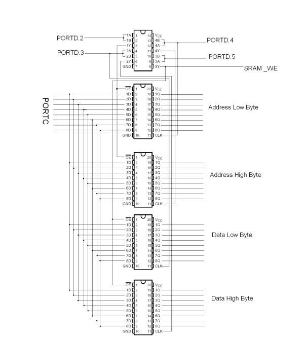
- The Mega32 MCU is used as the core of the hardware design. The MCU drives four octal buffers (SN74AHC574N). These buffers take input up to 5.5V, but can be run off a variable Vcc. We used 3.3V in this case so that it can interface with the rest of the chips and the actual Wonderswan.
- The octal buffers’ inputs are tied together, and we use control signals from the MCU to separately clock in each buffer. This allows us to drive a 32 bit wide bus with only an 8 bit wide data bus (PORTC) and some control signals. Two buffers send out a 16 bit address, and two buffers send out a 16 bit data word. Control signals are sent form PORTD of the MCU. There are four control signals ADDREN,DATACLK,ADDRCLK,WE corresponding to D.2,D.3,D.4,D.5 respectively. All control signals are connected to a 74AHC00 chip, which acts as a quad inverter. Non-inverted DATACLK and ADDRCLK are sent to the low byte buffers of data and address buffers respectively. The inverted versions are sent to their respective high byte buffers. This way, by clocking the signal to 1 and then to 0, we can write first to the low byte and then to the high byte. The inverted WE signal is sent to the SRAM chips and also to the output enable pins of the data buffers, while the inverted ADDREN signal is sent to the output enable pins of the address buffers.
- The outputs of the octal buffers are connected to two 8bit SRAM chips. These chips run off 3.3V and hold 32 kB of data each. Their address pins are tied together, so that they’ll provide 32768 words of 16bit each. This was done because the Wonderswan used a 16bit wide data bus.
- The buffers are tristate buffers, so the MCU can totally disconnect itself from the SRAM chips. This allows the SRAM chips to be connected to a Wonderswan without removing them.
- The memory chip’s data pins are also fed back into the MCU (PORTA and PORTB) so that the MCU can download and verify data uploaded to the SRAM chips.
- The memory chip’s data and address pins are also connected to the PCB card edge board for insertion into the Wonderswan. Consult the pin out specification for more information.
- All CMOS inputs that cannot be guaranteed a value because certain circuits have been shut off are pulled down to ground using 51k resistors for the buffers and 10k resistor packs for the SRAM addresses.
Parts list:
- STK-500: included
- Atmel Mega32: $8.00
- Two Solder Boards: $2.50*2=$5.00
- Two SRAM Chips: $4.99*2=$9.98
- Four SN74AHC574N Octal Buffers: $0.34*4=$1.36
- SN74AHC00N NAND: $0.32
- Various Passive Components (resistors, wires): included
- LM1117DT-3.3 3.3V Low Dropout Voltage Regulator: $0.74
- Blank PCB Board: $4
- Etchant Used (1/2 bottle): $2
- White Board: $5
- TOTAL: $36.40
For more detail: Wonderswan Development Cartridge Using Atmel Mega32