Summary of ATMega Control Board Manual V1.0 – Complete Setup and Guide
The ATMega Control Board is a microcontroller platform centered on the Atmel ATMega32, designed for real-time, embedded applications with extensive peripheral integration. It features 32KB flash memory, 2KB SRAM, and 1KB EEPROM, plus an 8-channel 10-bit ADC and a DS1307-compatible RTC with battery backup. It supports multiple communication protocols (USART, SPI, I²C, RS232 via MAX232), a 16x2 LCD interface, onboard buzzer, and power conditioning. The board includes hardware safeguards like watchdog timer and brown-out detection, and supports in-system programming with ISP tools for firmware updates. Its modular design aids prototyping and learning in embedded systems.
Parts used in the ATMega Control Board:
- Atmel ATMega32 microcontroller
- DS1307 real-time clock (RTC) module
- 24LCXX series EEPROM (external memory expansion)
- MAX232 RS232 level shifter IC
- 10-pin IDC header (ISP programming interface)
- DB25 connector (LPT port interface)
- Crystal oscillator (for external clock input)
- Analog-to-Digital Converter (internal to ATMega32)
- 16x2 or 20x4 character LCD module
- Contrast potentiometer (for LCD)
- Buzzer (audio signaling device)
- Power supply regulation and decoupling capacitors
- Reset tactile push-button switch
- LED indicators (for power, ISP activity)
- Trimpot (for LCD contrast adjustment)
- Multiple GPIO headers (digital and analog I/O)
The ATMega Control Board Manual describes an advanced microcontroller-based platform designed to facilitate high-speed, real-time and deterministic embedded processing in a resource-limited environment. The Atmel ATMega32 microcontroller, the primary processing unit, is based on an 8-bit Harvard RISC architecture with a maximum processing frequency of 16 MHz, giving a peak throughput of 16 MIPS. This supports tight loop control, real-time data acquisition and deterministic task scheduling.
Featuring 32KB of built-in self-reprogrammable (SR-Flash) memory, the system is well positioned to allow firmware re-flashing in-circuit and is capable of over-writing code on demand without the need for any external programming interface. In addition to the self-reprogrammable flash memory, the microcontroller’s memory map includes two additional memory options: 2KB of SRAM buffer for temporary variables, and 1KB of EEPROM memory for long-term, non-volatile storage of parameters—this is ideal for retaining parameters when the system turns off.
A built-in 8-channel 10-bit resolution analog-to-digital conversion subsystem allows the board to operate in analog-rich environments, where sensor inputs that are continuous-domain are converted to discrete digital values with a medium level of precision. Adding a battery-backed DS1307-compatible RTC interface adds temporal resolution for use in time-stamped data logging and for scheduling without requiring external time sources.
Peripheral extensions are provided, via a universally available GPIO header, for easily connecting passive and intelligent external modules. There is also a hardware RS232 transceiver for asynchronous serial comms to have the board function as slave, master, or peer in human machine interfaces (HMIs), supervisory control and telemetry.
2. System-Level Specification Matrix
Microcontroller Core Parameters:
Processor Unit: ATMega32 (Harvard RISC, 8-bit)
Clock Domain: Internal oscillator or external crystal; nominal 16 MHz
Code Memory: 32KB ISP Flash, programmable via external download interface
Volatile Memory: 2KB internal SRAM
Non-Volatile User Memory: 1KB internal EEPROM
I/O and Signal Handling:
Digital I/O: 32 lines, each individually addressable and connected to header terminals
Analog Interface: 8 differential ADC channels, 10-bit resolution
Timers: 2 × 8-bit + 1 × 16-bit high-resolution timers with prescaler options
PWM Outputs: Four channels for modulated signal generation
Comparators: On-chip analog voltage comparator for threshold-based logic
Communication Infrastructure:
USART: Full-duplex synchronous/asynchronous serial interface
SPI: Configurable as master or slave, supporting multi-device synchronous data exchange
RS232: Integrated TTL-compatible level conversion for PC/PLC interfacing
Peripheral Subsystems:
RTC: Socketed interface supporting DS1307 with external battery backup
EEPROM Expansion: 24XX series compatible socket for external memory extension
User Interface Elements: Trimpot-controlled LCD interface, on-board tactile reset switch, audio buzzer for real-time alerting
Power Subsystem:
Input Voltage: Regulated +5V with onboard decoupling capacitors and power conditioning
Power Indicators: LED-based visual diagnostics during power-up and ISP activity
Chapter 2 – Program Download:
This chapter comprehensively outlines the procedural framework required to program the ATMega Control Board Manual microcontroller using the provided development board and software tools. It focuses on hardware interfacing, safe setup practices, and execution of code transfer using a proprietary ISP utility.
Program Download – Computer and Board Setup:
Establishing a reliable physical and electrical connection between the control board and the host computer is essential before initiating program transfer. Stability of the supply voltage and correctness of port connections are emphasized to ensure safe and successful memory writing operations.
Technical Insights:
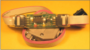
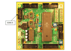
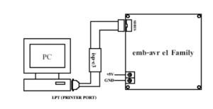
Establish the setup by aligning the 10-pin IDC cable with the SDBus socket located on the control board’s upper left section.
The grey DB25 connector is inserted into the computer’s parallel port; this serves as the communication bridge.
A regulated 5V DC supply must be applied to the board. The supply polarity must be accurate to prevent damage.
A red LED will indicate the board is powered. If unlit, verify the supply voltage.
Programming is initiated by launching the ISP utility from the CD-ROM. The yellow LED will turn on during active flashing.
Ensure SPI lines (PB5, PB6, PB7) are unoccupied or disconnected from other circuits to prevent bus contention.
Power supply current must meet the board’s programming load. Voltage drops below 5V may cause a programming failure.
Use the download speed slider in the programming software to reduce speed on faster computers for timing compatibility.
Installing and Running the Download Program:
In ATMega Control Board Manual this section details the setup and operation of the Mega32ISP software utility. The program allows selection of file, port, memory target, and download speed, followed by a structured approach for manual memory programming and verification.
Technical Insights:
Install the software from the CD-ROM using the setup utility. Compatible with all Windows-based systems.
Launch the ISP tool (Mega32ISP or mega32isp.exe) and select the correct communication port.
Adjust the download speed using the built-in slider to match your computer’s timing with the microcontroller.
Select the memory destination—usually Flash for code, EEPROM for stored variables.
Choose your compiled and error-free HEX file to be programmed.
Erase the microcontroller memory using the “Chip Erase” function, then verify memory is blank.
Click “Program” to initiate the memory write. The yellow LED will indicate active programming and a progress bar will display download status.
After successful flashing, use “Verify” to match memory content with the buffer and ensure programming accuracy.
Other Features of the Program Software:
Beyond basic programming, the ISP tool offers automation and protection features. This section describes advanced utilities such as Auto Mode, lock/fuse bit settings, and reading microcontroller identifiers, enhancing efficiency and safety in both development and manufacturing contexts.
Technical Insights:
Auto Mode automates repetitive programming steps, ideal for production lines: Open File → Erase → Blank → Program → Verify.
Lock bits can protect memory regions from overwrites or unauthorized access—read and configure them with caution via Info/Settings.
Fuse bits configure critical system-level settings such as oscillator type, bootloader size, and startup timing. Incorrect values may lock or disable the MCU.
Signature reads the 3-byte chip ID for device validation; Calibration reads a fixed oscillator tuning value (read-only).
While these tools offer enhanced control, users should refer to the ATMega datasheet before making irreversible changes.
Chapter 3: System-Level Reset and Hardware Safeguards:
Chapter 3 delves into the reset and hardware safeguard mechanisms of the ATMega Control Board Manual, highlighting the integrated reset circuitry, brown-out detection, and watchdog timer. These embedded features ensure system stability by mitigating low-voltage operation, preventing code lock-ups, and enforcing controlled reinitialization sequences.
Microcontroller Reset Mechanism:
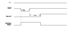
The ATMega Control Board Manual integrates an onboard tactile push-button interface explicitly designed to invoke a hardware-level system reset. Activation of this interface triggers an asynchronous reset vector execution sequence within the ATMega32 microcontroller, thereby forcing a reinitialization of the program counter and all hardware peripherals mapped via the internal I/O registry space. Upon release, a pre-defined debounce and stabilization interval ensures that transient voltage fluctuations are fully attenuated before the microcontroller resumes deterministic code execution. This reset mechanism reverts all I/O registers to their factory-defined power-on default states.
Brown-Out Detection (BOD) Subsystem:
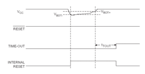
The embedded Brown-Out Detection (BOD) facility, internal to the ATMega32 silicon, serves as a voltage threshold monitoring subsystem tasked with ensuring operational integrity under fluctuating supply voltages. By configuring the BODLEVEL fuse bit, developers may define a deterministic cut-off voltage level—commonly 2.7V or 4.0V—below which the MCU will autonomously assert a system reset. Hysteresis behavior is architecturally implemented to mitigate rapid toggling in edge-voltage conditions, and a programmable recovery delay is imposed post-threshold reattainment to validate supply voltage stability before microcontroller reinitialization. Enabling this feature requires activation of the BODEN fuse during firmware upload or fuse programming operations.
On-Chip Watchdog Timer (WDT) Safeguard:
To safeguard against runtime code lock-up and errant infinite loops, the ATMega32 features an integrated Watchdog Timer (WDT) system. Once initialized, the WDT operates autonomously, invoking a microcontroller reset upon expiration of its internal countdown, unless explicitly refreshed via execution of the WDR (Watchdog Reset) instruction within a predefined interval. This mechanism is governed by a prescaler architecture embedded within the Watchdog Timer Control Register (WDTCR), offering programmable timing granularity across several orders of magnitude. The watchdog timer thus serves as a failsafe supervisory module, indispensable in autonomous and fault-intolerant embedded systems.
Chapter 4: Internal Memory Hierarchy and Address Mapping:
In ATMega Control Board Manual it outlines the ATMega32’s tripartite memory structure—SRAM for volatile data, EEPROM for non-volatile user settings, and Flash for program code. Detailed memory addressing and control mechanisms are discussed for efficient data and program management.
Overview of Memory Segmentation:
The ATMega32 microcontroller exhibits a tripartite memory architecture, comprising Static Random Access Memory (SRAM), Electrically Erasable Programmable Read-Only Memory (EEPROM), and Flash Program Memory. SRAM serves as a volatile workspace for dynamic data manipulation, Flash Memory hosts executable code with reprogrammability support up to 10,000 cycles, and EEPROM offers persistent non-volatile storage optimized for runtime calibration parameters and configuration constants.
SRAM Data Memory Architecture:
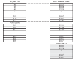
The SRAM module in the ATMega32 spans 2KB, segmented across a specialized memory map. The initial 32 bytes house the working general-purpose registers (R0–R31), directly addressable by most arithmetic and logic instructions. These are followed by 64 bytes of I/O registers interfacing internal peripherals. The remaining 2048 bytes are user-accessible SRAM, which supports five addressing modes: direct, indirect, indirect with displacement, indirect pre-decrement, and indirect post-increment—affording optimized access for stack operations, pointer arithmetic, and data streaming algorithms.
EEPROM Non-Volatile Memory:
The integrated 1KB EEPROM is accessible via a register-mapped interface including the EEAR (EEPROM Address Register), EEDR (EEPROM Data Register), and EECR (EEPROM Control Register). Write operations involve a staged transaction: the target address is loaded into EEAR, data into EEDR, and a control bit in EECR is set to trigger a write cycle. EEPROM read follows an analogous pattern with the control register toggled for read instead. Timing constraints—imposed by the write cycle’s internal charge pump—must be respected to avoid data corruption. Sample code and access routines are included in the official ATMega32 datasheet and the board’s bundled CD-ROM.
Flash Program Memory:
With 32KB of Flash memory partitioned as 16K × 16-bit words, the ATMega32 supports direct instruction fetches aligned to the AVR instruction set, which encompasses 16- and 32-bit opcodes. Its 14-bit program counter provides complete linear addressing without the need for page register management. A dedicated boot flash section facilitates self-programming routines through UART-mediated bootloaders. These routines enable firmware upgrades via serial communication without necessitating external programmers, contingent on proper fuse bit configuration for BOOTRST and BOOTSZ.
Chapter 5: Microcontroller Port Functionalities and Pin-Level Architectures:
This section covers the functionality of all I/O ports (PORTA–PORTD), including digital I/O and peripheral interfaces such as ADC, SPI, UART, PWM, and interrupts. Each port’s multiplexed roles and electrical characteristics are described in detail.
General Overview of Port Subsystems:
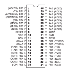
The ATMega32 includes four general-purpose I/O ports—PORTA through PORTD—each comprising 8 bidirectional lines capable of acting either as digital I/O or as multiplexed signal lines for peripheral modules. Control over directionality and data state is maintained via DDRx, PORTx, and PINx registers. Advanced peripheral functions—such as SPI, TWI (I2C), ADC, PWM, and UART—are contextually multiplexed over these physical pins, necessitating proper configuration of their corresponding control registers.
PORTA – Analog and General-Purpose I/O:
PORTA serves as both a general-purpose digital interface and the analog signal input bank for the onboard ADC subsystem. Each pin can independently assume high-impedance input, active-high output, or open-drain output configuration. Digital write operations are conducted via PORTA, while DDRA defines pin directionality. Cumulatively, the port can source or sink up to 200mA, allowing direct LED driving under current-limited conditions. Ground references are provided in parallel with signal lines to ensure signal integrity across capacitive or inductive loads.
PORTB – SPI, Analog Comparator, and Timer Extensions:
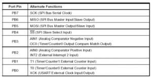
PORTB supports advanced digital functionality including:
PB7–PB5: SPI Clock (SCK), MISO, MOSI
PB4: Slave Select (SS)
PB3–PB2: Analog Comparator inputs
PB1–PB0: Timer/Counter and external event inputs
Port B’s multiplexed architecture requires the SPI subsystem or comparator to be explicitly enabled via SPCR or ACSR registers to override digital I/O behavior.
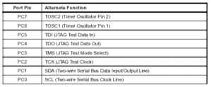
PORTC – JTAG, I2C, and External Clock Interface:
PORTC incorporates dedicated hardware interconnects for:
PC7–PC6: Crystal Oscillator input (RTC reference)
PC5–PC2: JTAG boundary-scan debugging interface
PC1–PC0: TWI/I2C master-slave communication
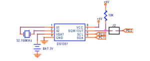
On the ATMega Control Board, PORTC is pre-wired for integration with the DS1307 RTC and external EEPROM via I2C, enabling both timekeeping and data persistence functionalities without MCU load.
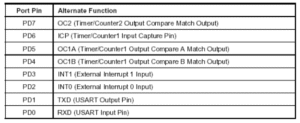
PORTD – External Interrupts, UART, and PWM Control:
PORTD is extensively used for asynchronous communication and interrupt handling:
PD7–PD4: PWM output channels
PD3–PD2: External interrupts INT1 and INT0
PD1–PD0: UART TXD and RXD, interfaced to MAX232 for RS232-level signaling
This port handles both real-time input signaling and outbound pulse-width modulation, making it critical in both data and actuation paths of the control system.
Chapter 6: Serial Communication via the Two-Wire Interface (I²C):
The chapter focuses on the two-wire I²C protocol used for connecting peripherals like the DS1307 RTC and 24LCXX EEPROM. It explains address structuring, data transfer formats, and read/write operations for reliable serial communication.
Protocol Overview:
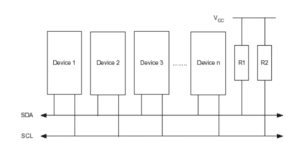
The I²C (Inter-Integrated Circuit) bus is a two-wire serial protocol that supports master-slave device topologies, enabling up to 128 uniquely addressable nodes on a shared data/clock bus. Only one node can function as master at any time, orchestrating clocking and data flow. The ATMega32’s TWI hardware module abstracts the complexities of bit-banging, enabling interrupt-driven communication sequences conforming to the I²C standard.
Pull-up resistors are necessary on both SDA and SCL lines to stabilize the bus when idle, typically using 4.7kΩ to 10kΩ values depending on bus capacitance and clock rate.
Interfacing the DS1307 RTC:
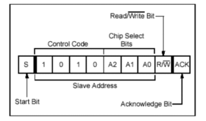
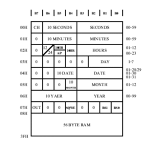
The DS1307 employs a standardized I²C address (1101000 binary), with time and date parameters stored in BCD-encoded registers. Transactions begin with a write sequence to set the register pointer, followed by either a data write or read command. Internal scratchpad RAM (56 bytes) is also accessible for temporary variable retention. Stop conditions must be accurately terminated per I²C protocol to finalize communications.
24LCXX EEPROM Interfacing:
The 24LCXX series of EEPROMs (e.g., 24LC128) function similarly to the DS1307, with a base I²C address of 1010 followed by A2–A0 configuration bits. The memory map supports:
Byte Write: Single-byte address and data payload
Page Write: 64-byte burst transfer with automatic internal address incrementing
Random Read: Target register address write followed by read phase
Sequential Read: Continuous streaming read, address auto-wrap on overflow
Data consistency relies on strict adherence to clock stretching, page boundary limits, and internal write-cycle timing.
Chapter 7 – ADC
Introduction:
Embedded within the architecture of the ATMega32 microcontroller lies a sophisticated 10-bit successive approximation analog-to-digital converter (ADC), interfaced with an 8-channel multiplexer that permits the selection of eight discrete, single-ended analog inputs. These channels are multiplexed through PORTA, necessitating a deliberate configuration during initialization to designate specific pins for analog input functionality versus digital I/O operations. With conversion latencies ranging from 65 to 260 microseconds, precise timing control is imperative to ensure data integrity, as premature access to ADC registers can yield invalid digital outputs, a phenomenon well-illustrated through the exemplar routines included on the accompanying CD-ROM.
Voltage Reference:
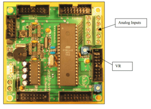
The ADC module provides dual-reference voltage modalities: internal and external. Internally, users may select between a fixed 2.56V reference or the AVCC rail voltage (typically aligned with Vcc). Atmel specifies a constraint ensuring AVCC remains within a 0.3V differential from Vcc for optimal performance. Externally, the reference input is facilitated through the AREF (pin 32), with a voltage-adjustable VR module on the control board offering fine-tuned calibration spanning 0 to 5V. It is critical that analog inputs do not exceed the configured reference voltage, as full-scale output (0x3FF) corresponds to an input precisely matching the reference.
Connecting to the ADC Terminals:
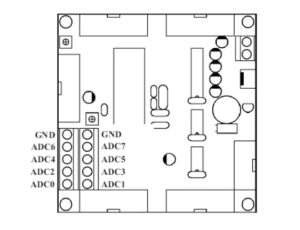
For signal acquisition, analog sources should be interfaced with the green terminal blocks specifically provisioned for ADC inputs. The design consciously separates analog and digital grounds to suppress interference and mitigate ADC noise susceptibility. Users are strongly discouraged from employing PORTA’s digital headers for analog interfacing, preserving signal integrity via dedicated analog grounding.
Performing an A/D Conversion:
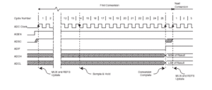
Activation of the ADC subsystem is accomplished by setting the ADEN bit in the ADCSRA control register. Voltage reference selection and input channel assignments are only latched upon enabling the ADC. Conversion results are stored across ADCH and ADCL registers, typically right-justified unless the ADLAR bit in the ADMUX register is asserted. An interrupt flag signifies completion, and polling this flag is the recommended synchronization method prior to register access. A detailed timing diagram for single-channel acquisition is provided in the documentation.
Chapter 8 – LCD:
Introduction:
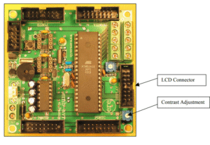
The ATMega Control Board Manual accommodates a parallel character LCD interface via a pre-configured header, supporting standard LCD modules (e.g., 16×2, 20×4) for real-time status feedback. A contrast potentiometer is integrated into the board architecture to modulate the display’s legibility. Provisioning of +5V on pin 16 supports LED backlighting functionalities on compatible displays.
Operation of the LCD:
Data interfacing is optimized via a 4-bit parallel mode wherein each byte is bifurcated across two sequential transmissions, effectively halving the required data lines. Data pins D4 through D7 are mapped to PORTC (PC4-PC7), while RS and E control signals are wired to PC2 and PC3, respectively. The R/W line is tied low, rendering the interface write-only. Backlight connections (BL+ and BL-) are made through pins 16 and 15, regulated via an inline current-limiting resistor whose value may be adjusted to calibrate brightness.
Connection of the LCD:
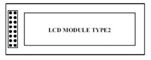
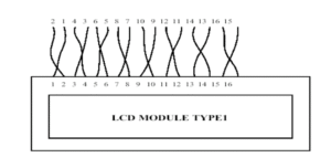
Two physical connector configurations are supported: dual-row 8-pin (Type 1) and inline terminals (Type 2). For dual-row layouts, IDC connectors with ribbon cables ensure seamless mating. For inline LCDs, each ribbon wire must be manually cross-referenced to the corresponding LCD terminal, adhering to strict polarity and pinout verification procedures to avoid miswiring. Proper orientation of the IDC header and verification of power lines are emphasized to prevent irreparable damage to the LCD module.
Chapter 9 – RS232:
Introduction:
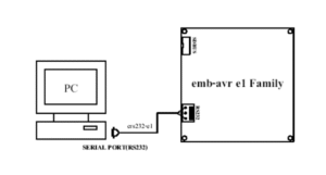
The ATMega32 integrates a Universal Synchronous and Asynchronous Receiver Transmitter (USART), enabling serial communication with external systems via RS232 protocol. This facilitates real-time data exchange with host systems such as PCs for command execution or telemetry logging within user applications.
Connecting to the RS232 Port:
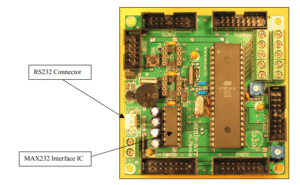
Due to voltage level discrepancies between TTL (+5V) logic and RS232 standards (+15V), a MAX232 transceiver is employed to bridge the signal domain. A polarized 3-pin header allows secure connectivity, with RX and TX lines cross-wired to accommodate transmission conventions. Continuity testing with a multimeter is advised prior to first-time connection.
 Computer Programs and other Options:
Communication initialization can be executed through standard terminal software (e.g., HyperTerminal), or programmatically via high-level languages such as Visual Basic utilizing MSCOMM ActiveX controls. Baud rate, parity, and stop bit configurations must mirror those programmed into the ATMega’s USART control registers. The microcontroller’s datasheet provides exhaustive configuration detail essential for robust serial interfacing.
Chapter 10 – Buzzer:
Introduction:
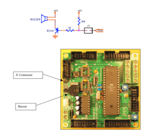
The onboard buzzer serves as an acoustic signaling mechanism, capable of producing tones of variable frequency and duty cycle to indicate events ranging from status alerts to critical warnings.
Using The Buzzer:
The buzzer is activated through digital high output on PD4. A logical low on PD4 will deactivate the audio output. For applications requiring PD4 reallocation, the J1 jumper may be disengaged, effectively decoupling the buzzer from the port pin and preserving I/O resource availability.
Chapter 11 – Power Supply:
Requirements:
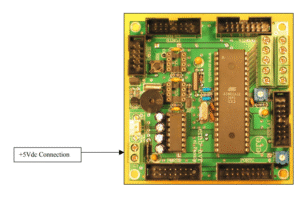
The ATMega Control Board Manual necessitates a regulated +5V DC input for stable operation. Although quiescent current demands are minimal, attached peripherals can significantly escalate power requirements. A supply exhibiting both low ripple and sufficient current headroom is essential to avert under voltage-induced resets and ensure consistent performance across varying load conditions.
Conclusion:
The ATMega Control Board Manual, underpinned by the robust capabilities of the ATMega32 microcontroller, presents an exemplary embedded platform engineered for both instructional and industrial applications. Through its integration of a wide array of peripheral modules—including ADCs, EEPROM, RTC, LCD interfacing, RS232 communication, and onboard watchdog and brown-out protection—it effectively demonstrates the holistic convergence of analog and digital system design. The modular structure and logical layout of ports A through D, coupled with the inclusion of power conditioning, real-time interrupt handling, and advanced memory segmentation (SRAM, EEPROM, and Flash), render it highly adaptable for real-time data acquisition, user interface display, and serial data exchange with host systems. Furthermore, its programmable architecture, combined with accessible development utilities and sample firmware, significantly lowers the barrier for prototyping and system debugging. Altogether, the board serves as an ideal educational and developmental scaffold for mastering microcontroller-based design, emphasizing reliability, expandability, and control precision.
Read more : ATMega Control Board Manual V1.0 – Complete Setup and Guide



 Computer Programs and other Options: