Summary of NES EMULATION USING ATMEGA32
This project aimed to recreate the Nintendo Entertainment System (NES) CPU using Atmel microcontrollers by emulating the modified 6502 processor and generating compliant NTSC video output via an AD724 chip. Audio processing and full NES Picture Processing Unit (PPU) video generation were excluded due to complexity. The team focused on cartridge reading, controller input, memory-mapped I/O synchronization, and the emulation of all 6502 instructions, registers, and addressing modes. Timing synchronization with the original NES CPU clock was carefully managed through optimized code techniques.
Parts used in the NES Emulation Project:
- STK500
- 72-pin Edge Card Connector
- AD724 (RGB to NTSC converter)
- ELM304
- UART Cable
- 2 Breadboards
- Large Solder Board
- 3 Crystals
- Resistors and Capacitors
- Wires
- Protoboard
- Color TV
- NES Controller
- Power Supply
- MCU Socket
- Machine Pins
- 2 Controller Sockets (Parallax NES Controller Socket)
- SOIC pad
- 2 AtMega644 microcontrollers
OVERALL DESIGN GOAL
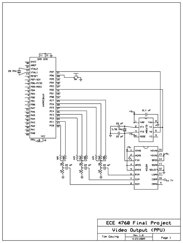
The overall goal of our project was to recreate the Nintendo Entertainment System (NES) using Atmel Microcontrollers. We decided early on the adding audio to the mix was likely going to be too much work in the time that we had to complete the project. Therefore, we decided to leave all audio aspects out of the mix. Therefore, our focus became emulation of the modified MOS6502 processor that the NES used as the CPU and the generation of the video. It was determined, however, that the video generation that was done by the Picture Processing Unit (PPU) was too complex to be entirely done in software, or even used limited hardware (See below for a discussion on the methods of the NES PPU). Therefore, what remains of our project is the 6502 emulation, cartridge reading, controller input, and memory mapped I/O synchronization. The lack of video, however, was not something that we wanted to settle with, so we decided to show off some of the video tactics that were utilized by the Nintendo. Our video outputting scheme must fully comply with NTSC standards. We achieved this compliance by using a specialized chip (AD724) to convert Red/Green/Blue into NTSC.
Development of the NES 6502 Emulation
The 6502 was an evolutionary microprocessor that was widely used for one reason: it was absolutely dirt cheap compared to the rest of the functional microcontrollers on the market. The modified version of the 6502 that the NES uses was also quite cheap to produce, which is why ten years after production of the product Nintendo was still asking for the far outdated 6502. The main differences between the two chips involve the I/O line designations as well as the addition of the pseudo-Audio Processing Unit (pAPU). The added I/O lines include five that are devoted to obtaining data from the controllers and two that are used as audio output channels.
The interesting part of the NES 6502’s operation is that there were absolutely no additions to the instruction set available to the programmers of the NES games. The raises the obvious question: how does one read from the controllers or generate the newly supported audio? The answer to that lies in the memory mapped IO which is the basis for nearly all communication on the NES.
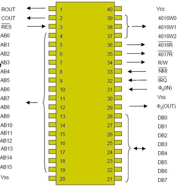
The memory-mapped IO is a series of memory addresses which, when written to or read from, produce side effects in other aspects of the hardware. The basic set of IO ports are listed below, and it should be noted that additional IO ports can be added via use of Memory Mapping Chips (MMCs) which would be hardwired into the game cartridge to expand the capabilities of the NES. (This project does not deal with interfacing to any particular MMC but rather passes most all addressing out to the cartridge where any present MMCs are given the opportunity to react to the programmed signals. Therefore, we will not discuss the MMCs any further, but point interested parties to the references at the end of the document.)
The registers listed above are merely “views” at data registers contained within other hardware (PPU registers being hardwired address correlations to the video processor and audio registers being internal latches in the NES 6502 that output to specific audio generating hardware. These registers will be referenced directly in points hereafter, at which time the uses of all imperative registers will be explained.
Of course, behind the intertwined hardware and IO connections, at the heart of the NES 6502, is the slightly modified version of the original 6502, and therefore emulation of this hardware is the forefront of the project.
The general method of emulating a processor is to completely replicate the functions of each individual operation that the processor can handle. The 6502, while the 8 bit opcode could support up to 256 instructions, only 151 of the 256 available opcodes has defined behavior (In fact, using other instructions opcodes not necessarily produce no operation, but may in fact send your program into complete disarray.) Furthermore, these 151 opcodes only actually support 56 distinct operations, with specific opcodes merely varying the addressing mode utilized by the operation (see addressing modes below).
Along with successful emulation of all instructions, we must establish successful emulation of all registers. The registers present on a 6502 are as follows:
- Program Counter (PC): 16-bit pointer to the next instruction to be executed.
- Stack Pointer (SP): 8-bit pointer into the stack.
- Accumulator (A): The key arithmetic register for nearly all operations.
- Index Register X (X): A register typically used for indexing and counting. Additionally can be used to stack pointer transfers.
- Index Register Y (Y): A register typically used for indexing and counting.
- Status Register (S): Contains flag pertaining to the preceding operation.
Status Register Layout (Bit7 – Bit0)
N | Negative |
V | Overflow |
– | ignored |
B | Break |
D | Decimal (use BCD for arithmetic) |
I | Interrupt (IRQ disable) |
Z | Zero |
C | Carry |
(Note that the modified 6502 used in the NES did not support BCD mode, but did not bother to remove the opcodes that set and clear the flag, therefore providing another conditional flag which can be set and branched upon at will.)
Of the above registers, the only one that requires more than a variable in the program is the stack pointer. Along with the stack pointer is the need to implement a stack directly into the data memory of the Atmega644. For the NES, this stack was located in the memory, addressed from $100 to $1FF. In addition, the 6502 did not contain and safeguards on the length of the stack, and if one was to push over 256 elements onto the stack, they would wrap around and start trashing the lower bytes of data. In emulation, in is not pertinent to worry about this overflow either because this fact is known by the programmers and was either avoided, or in extremely rare cases, used to the programmers advantage.
The available opcodes operate on the aforementioned registers. They are broken down into a few sets of operations:
- Load / Store Operations
- Register Transfers
- Stack Operations
- Logical Operations
- Arithmetic Operations
- Increments & Decrements
- Shifts
- Jumps & Calls
- Branches
- Status Flag Changes
- System Functions
For a full list of operations, see the table at the end of the document.
Emulation of the 6502 requires working with the 13 different addressing modes. These addressing modes work as follows:
Implicit
There are many instructions in the 6502 processor that have “implicit” targets, such as “Clear Carry Flag” (CLC) and “Set Interrupt Disable” (SEI), meaning that the operation is only defined to work at those specific points. This allows implicit instructions to take up only one byte of program memory.
Accumulator
Accumulator addressing means that the instructions work directly upon the accumulator register. In a sense, these are also implicit by nature, with the only exception being that the implicit address is always the same.
Immediate
Immediate addressing allows the use of an 8-bit immediate offset by the programmer directly in the code itself. Instructions using immediate addressing take two bytes of memory.
Zero Page
Zero Page addressing mode is the most efficient way of accessing actual memory. Addressing in this manner simply means that the address is located in memory $00XX, and therefore will only take two bytes of memory because only one 8-bit address is required for addressing.
Zero Page, X
Zero Page, X addressing will essentially restrict your memory field to only the first page of memory (256 bytes). It first takes the zero page address and then it adds the X register to it to produce a 8 bit address. Note that the address cannot exceed 8 bits, and therefore will always wrap around from $FF to $00 rather than $100 (which of course is no longer on page zero of memory). Like Zero Page, this is a two byte instruction.
Zero Page, Y
Zero Page, Y is essentially the same as Zero Page, X except that the two are not interchangeable. The only instructions that use Zero Page, Y are the LDX and STX instructions, load and store X register to/from memory. The only reason that Zero Page, Y is used rather Zero Page, X is because the instructions cannot modify the contents of X. Also a two byte instruction.
Relative
Relative addressing is used for branching. It specifies the value which should be added to the PC upon a true evaluation of the branch condition. This is a two byte instruction.
Absolute
Absolute addressing is when a full 16 bit address is provided ( LSB first) in the two bytes following the opcode. The specified address is a direct lookup into the memory.
Absolute, X
Similar to Absolute addressing, Absolute X addressing provides a 16 bit address, but additionally adds the value of the X register to it before accessing the memory.
Absolute, Y
Identical to Absolute X, replacing the X register with the Y register. (Three byte instruction)
Indirect
Indirect addressing is only used by jump commands. Essentially, the two bytes after the opcode specify an address in memory which contains the LSB of another 16 bit addressing. It is this address that is the desired destination of the jump instruction.
Indexed Indirect
Indexed Indirect addressing adds the X register to the supplied 16 bit address and then works exactly as Indirect addressing works.
Indirect Indexed
Indirect Indexed addressing retrieves the 16 bit value stored at the address specified in the two bytes following the opcode. It then adds the Y register to the retrieved 16 bit value and uses this value as the jump location.
Emulation
Now to discuss how the 6502 was specifically emulated. The main goal is to obviously recreate program control, but the real catch is that we need to maintain control of the timing elements native to the NES 6502. The NES cpu ran on a 1.79 MHz clock, which compared to the 16 MHz clock we used for the Atmega644, gives us approximately 8.5 cycles per native 6502 instruction. Yet there is still an added bonus to this because the 6502 ran on a base 2 cycle system, meaning that no instruction took fewer than 2 cycles, and some took as many as 7 cycles to complete. This means that our base timing level is at 17 cycles. Now if the 6502 had only 2 cycle instructions then we would need to improve the speed of the program in a few places. However, if we amortize the time taken by a series of instructions in general we are looking at a very well balanced and time synced emulation.
This is all made possible via a near exclusive use of #define coding style. Working in this manner, while it does make the code significantly larger due to the replication of code in many places, it saves a bunch of instructions on every single operation. We also need to be careful when working with code in this manner. When using #defines as a method of increasing the speed of the code, then you must try to only pass in either a single variable or an immediate variable into them. If you are careless in their use, you may end up replicating code along the lines of variable increments or memory lookups. These kinds of bugs also manage to hide themselves to a level of total obscurity due to the similar appearance of a function and a #define.
First, we grab the opcode from the cartridge (The first address of the program is addressed inside of the cartridge at $8000.) and use that as an offset for a jump command. This jump is done by executing the jumper function. We use a function for this because we need to gain access to the internal program counter. We do this by popping two bytes off the stack which by the nature of function calls is the program address to which the function will return. We then add the opcode to this value two times to account for the fact that a jump instruction occupies two words in memory. The result is pushed back onto the stack and the function is allowed to return to the desired place within the jumplist. This jump command will land us somewhere in the jumplist, which is 256 consecutive jump commands. These jump commands will direct our program to individual sections that handle each instruction.
At these commands, we need to indicate three things. First, we need to indicate the size of the instruction in bytes. Secondly, we need to indicate the addressing mode which is used. And, finally we execute the actual instruction which the opcode specified.
Indicating the size of the instruction is a simple enough operation. The instructions can be either one, two, or three bytes. The first byte is the opcode, so if the operation only needs one byte, then we are already done at this point. If the operation requires any more bytes, then we must retrieve a few more bytes from the cartridge. These bytes are stored into the instr_byte array (in the 1 and 2 positions, because the opcode takes instr_byte[0]) and are used in determining addressing.
In order to accurately setup the addressing methods and to allow the addressing modes to exist completely independent of the instructions that are calling them, we need to define a few variables which will consistently be used, no matter what the instruction is. This allows us to keep all of our code inside of the main function and makes the #define method more efficient. While functions would clearly clarify the code, getting into and out of the functions would waste far too much time. The variables that we used were rOP(char) and rOPA(int), named for operand and operand address. Essentially, most addressing modes have both an address setup routine as well as an extraction routine. The address setup routine places the address which we intend to work upon into rOPA. The extraction routine, internally calls the addressing routine and retrieves that value from the address in rOPA, storing it into rOP.
As stated before, prior choice of rOP and rOPA make almost all other instructions easy to implement by simply working with the value in rOP or rOPA. The exceptions to this are rotate shift operations, which need a post-step to place the value back into memory or reapply rOP to the accumulator, depending upon the addressing mode. All other instructions, after making a call to an addressing routine, simply make a call to the actual instruction routine that was indicated and it will be carried out. Once completing this, it jumps back to top of the program to grab a new instruction.
As I mentioned previously, most instructions involve obtaining a value from memory. Yet, these memory addresses refer to the memory actually present on the NES. Where exactly is that memory going to reside considering we need to maintain stack space for the emulation to run within. Initially, this looked to be an issue because the memory addresses were 16bit addressable, meaning 64K of memory.
Parts List:
Item | Cost | Vendor | Part # |
STK500 | $15 | N/A | N/A |
72-pin connector | $2 | Electronic Surplus | 72-pin Edge Card Connector 0.1� |
AD724 | Sample | Analog Devices | AD724 |
ELM304 | $6.50 | ELM | ELM304 |
UART Cable | $1 | N/A | N/A |
2 Breadboards | 1 Free, 1 $6 | N/A | N/A |
Large Solder Board | Free | N/A | N/A |
3 Crystals | $3 | N/A | N/A |
Resistors, Caps, etc. | Free in lab | N/A | N/A |
Lots of Wire | Free | N/A | N/A |
Protoboard | $4 | N/A | N/A |
Color TV | Free (previously owned) | N/A | N/A |
NES Controller | Free (previously owned) | N/A | N/A |
Power Supply | $5 | N/A | N/A |
1 MCU Socket | $0.50 | N/A | N/A |
5 Machine Pins | $0.25 | N/A | N/A |
2 Controller Sockets | $4 | Parallax | NES Controller Socket |
SOIC pad | $1 | N/A | N/A |
2 AtMega644�s | Free Sample | AtMega | |
Total | $48.25 | N/A | N/A |
For more detail: NES EMULATION USING ATMEGA32