I’m thinking about a new project, something a little unusual but still with a rich history of information upon which to base the build. On Tindie, I found the RC2014 project which is a build of a Z80 platform but based on some modern components. That got me thinking. My next project must be a Z80 based project.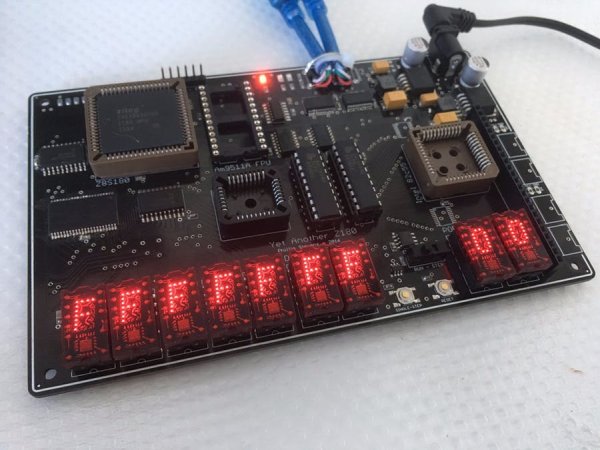
Why the Z80? Well, it was at one stage the most used CPU in the world, which leads to the great depth of information and experience available for designs, hardware, and software. Technically, it is advanced enough to avoid the need for a large number of ancillary chips, multiple power supplies, and multi-phase clocking that the 8008, 8080, and other older chips needed, but still it is complex enough that in doing a project I’ll feel like I’m actually building a computer.
This year marks 40 years (yes 40 years, since launch in July 1976) of the Z80, and still as a design and platform it looks like it will continue to be relevant into the future. So rather than building yet-another-ARM project. It looks like I will be marking the 40th anniversary of the Z80 with a new build.
As an outcome I’d like the solution to be able to interact with modern interfaces such as I2C, Ethernet, SPI, and USB, with access to a large physical memory space, with great performance, and yet retain the ability to be a single-step-able experimental platform with LED bus indicators. Single stepping is something that you can’t do with an Arduino, and it is a real differentiation.
Whilst it would be attractive to design in some old-school 1970’s devices, like the Am9511A Floating Point Unit (FPU) or an Intel 82C55 Programmable Peripheral Interface (PPI) device, in light of today’s environment they wouldn’t contribute very much to the outcome. Never-the-less, because they will add significant retro-chique to the outcome, they’re in!
Also, there is a temptation to build a CP/M system with full disk management. But again there are plenty of CP/M systems around. I’d like to build something more of an embedded platform, that doesn’t require mass storage to run applications.
It would be good if most of the basic interfaces could fit on one board, to avoid the need to build address and data bus extension. I think this will simplify the design significantly.
Processor Selection
The Z80 has been built continuously for 40 years, and in that time many manufacturers have produced silicon and several clones have been created. The Z80 range been continuously improved through the Hitachi 64180, to the Zilog Z180, and the Zilog Aclaim eZ80 devices. Each increment has integrated more accessory components, and improved the instruction throughput, as well as increased the clock rate.
Looking at the options available, the original Z80 requires logic to get started. So rather than building serial ports and timers, it looks like the Z180 might be the right place to start. So why not go all the way to the eZ80? Well the eZ80 is not dissimilar to an AVR ATmega device, with all of the system components integrated into the one device. Using an eZ80 CPU wouldn’t be like building a computer at all. It would be much more like building an Arduino, and I’ve been there already.
Out of the Z180 options, I would select the Z8S180 (at 33MHz) because it integrates sufficient material to get started (Timers, Interrupts, MMU, & USARTs), and leaves me the option to add complexity as I get going.
Memory Selection
A little research on the processor and available memory provides me with some cornerstones for the design. I will use Flash memory for the program storage, and static RAM for the system memory. Historically, UV erasable PROM and dynamic RAM would have been used. One advantage of static RAM is that the solution is fully single-step-able. Meaning, I’ll be able to watch the address bus and data bus process each instruction as the Program Counter marches along.
The Z180 can address up to 1MB of physical address space, and it makes sense to provide the full physical memory possible. The price of 1MB of SRAM or of 256kB of Flash is almost nothing these days. As the Z80 logical address space is only 64kB, the Z180 has an inbuilt MMU to manage its physical memory to logical memory mapping.
Frequency Selection for CPU
The best flash we can get easily is 55ns timing. This is bettered by SRAM, with 45ns. Converting this timing to a bus frequency we can achieve 20MHz or slightly better, but allowing for some buffering or address logic delay it would be better to keep the system bus under 20MHz.
Using this system bus speed of approximately 20MHz then poses a question; which is the right speed? Some references point out that the Z180 is very poor at holding the correct USART rate when the CPU clock is not a magic multiple of the USART rate. This is the same issue that the AVR ATmega device faces when its USART is not driven by a magic frequency clock. Therefore, lets us set the CPU clock to 18.432MHz, being most appropriate magic frequency for the following design.
The Z180 crystal clock can generate either doubled, or halved system clocks from the base rate. Starting with 18.432MHZ CPU clock, the system bus clock can be halved, and operated at 9.216MHz as needed. This is slow enough to allow most peripherals to interact with the CPU. Internally, the clock can be doubled to operate the CPU at 36.864MHz. This rate is slightly overclocking the Z180, but that’s what we live for. We don’t build slow computers.
Hardware Design Notes
Well quite a few iterations on my aspirations and thoughts have resulted in a YAZ180_v1 schematic, that I think is now basically frozen. Some of my design decisions follow.
After deciding not to use the TIL311 LED display devices because they are not easily obtainable, I found the alternative solution using the DM9368 display driver chip and LED display devices was very consuming of space on the board. Since the board had to be no greater than a maximum of 10cm by 16cm I decided to buy some TIL311 devices in advance, and then with the comfort of stock in hand I could use them for the design. Also, they add significantly to the retro-chique.
I would have loved to add the Wiznet W5300 device to the design to provide high speed Ethernet capability, but with a 100 pin VLSI it was just too complicated for the initial design. Next time.
I added a 82c55 interface chip. Knowing that it is very slow, requiring wait states to drive it, is one thing. But the advantage of having multiple latchable input and output ports, off one fairly compact integrated device made up for that problem. As it is a 1970s device it is also retro-chique accretive.
Designing using CUPL and the Atmel PLDs is in my opinion much simpler than tracing schematics and thinking through 7400 series NOR, NAND gates to get the desired addressing logic. Writing the logic in “c” like syntax is much less taxing on the brain.
After deciding to implement no bus drivers, and then building a solution adding drivers and termination to every address and data line, I have rationalised down to bus drivers on data, lower address, and control lines. These are the few lines that appear on all memory and I/O devices, and are taken to every point on the board. The upper address lines only appear on the PLD, SRAM, and Flash, which are very low load modern devices, so there is no point to buffer them. Using ABT logic limits the differential delay on the address lines to 2 ns, and since the read and write select lines are also buffered, there is no issue timing issue created.
Change the SN74ABT244 for the SN74ABT541. The only difference is the pin ordering, with the 244 being optimal for counter-flowing signals, and the 541 being optimal for unidirectional signals (physically). This will help layout.
Getting 20 address lines and 8 data lines to appear on the SMD SRAM memory is challenging. I will probably reassign the address lines to suit the Z8S180 pin-out, rather than spending hours untangling the lines. It won’t be too easy to do this with the Flash device, but as it is in a PLCC through-hole socket it comes inherently with “vias” making reaching it half as hard as SMD.
Input pin and I/O pins on Z8S180 include weak latch circuits to prevent excessive current draw by the receiver, if the pin is not externally driven. External pull-up or pull-down resistors should not be less than 15 kOhms to ensure that the resistors can control the state of the latch when power is supplied.
The screen grabs below show the board with the Vcc Layer in Grey, and GND Layer in Green. I have added some basic traces on those layers to close off the routing, which are misleading. The layers are actually completely filled, normally, as can be seen below.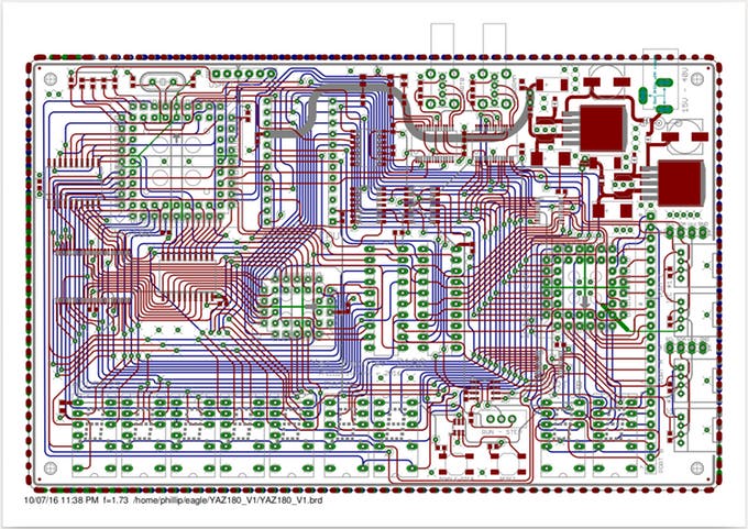
For more detail: Yet Another Z180 (YAZ180) Project