Summary of Advancements in Networked Biometric Authentication Systems
This article details a networked biometric authentication system designed for secure doorway access. It utilizes an ATMega32 microcontroller to interface with a capacitance-based fingerprint scanner, storing data in external SRAM before transmitting it via USART to a serial-to-Ethernet converter for server-side processing. The system employs Gabor filtering and minutiae comparison for verification, achieving a compact 9"x9" board at a cost of $75.
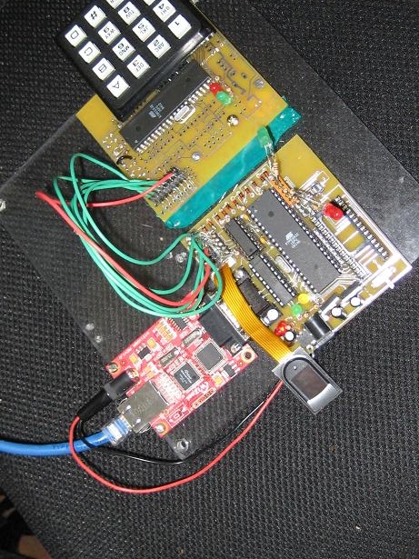
Parts used in the Networked Biometric Authentication System:
- ATMega32 microcontroller
- FPC1011C capacitance-based fingerprint sensor
- Parallel SRAM
- WIZ110SR serial to Ethernet converter
- Alphanumeric keypad
- LCD display
- Custom-designed PCB board
- LED indicators
- Client PC server computer
Introduction:
With the growing imperative to safeguard data and premises, the biometric authentication sector is witnessing significant market expansion. Our endeavor focuses on creating a scalable, compact, and efficient device tailored for securing doorways within a complex. Leveraging a FingerPrint Cards capacitance-based fingerprint scanner, our system employs an ATMega32 microcontroller for data capture, storing the data temporarily on external SRAM. Subsequently, the data is transmitted through the microcontroller’s USART serial port to a serial to Ethernet converter, enabling communication with a server computer for filtering and authentication processes.
High-Level Design:
Rationale
Amidst escalating security concerns across military, corporate, and personal domains, the biometric authentication realm emerges as pivotal. This sector, which generated approximately US $3.01 billion in revenue in 2007, is projected to soar to US $7.41 billion by 2012, with fingerprint authentication alone expected to hit US $400 million by 2010. Driven by the exigency to fortify data and premises effectively and spurred by the burgeoning market trajectory of the biometric industry, our project endeavors to devise a system employing fingerprint biometric authentication for doorway access.
Fingerprint Capturing
To capture fingerprint images, our system instructs the microcontroller to await available characters in the USART. Upon receiving the character ‘G’, the microcontroller initiates image capturing. Subsequently, the system reads the stream from the fingerprint reader, concurrently storing data points in SRAM and integrating them into Ethernet packets for future transmission. The matching result is then displayed via LED indicators. Upon transmitting all 30400 bytes, the microcontroller reverts to standby mode.
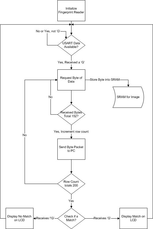
Logical Structure of Fingerprint Capturing Process:
Fingerprint Verification and Background Math:
Fingerprint matching entails three primary steps: feature enhancement, minutiae extraction, and minutiae comparison. Feature enhancement involves filtering to accentuate fingerprint features, followed by minutiae extraction to identify legitimate features. Finally, minutiae comparison juxtaposes identified minutiae against reference minutiae in the database to ascertain authentication.
Step One – Feature Enhancement:
Normalization standardizes grayscale values of the input image based on preferred mean and variance, enhancing feature visibility. Gabor filtering further refines image quality, applying directional filters incrementally to accentuate ridges. Threshold binarization categorizes pixels as ridge or valley based on average pixel values in respective windows, followed by thinning to refine ridge representations.

Step Two – Minutiae Extraction:
Minutiae, comprising ridge endings and bifurcations, are identified using a 3×3 window to compute crossing numbers. Subsequently, spurious minutiae are eliminated, considering proximity to image borders or low variance regions.
Step Three – Minutiae Comparison:
Minutiae comparison aims for simplicity and accuracy, identifying transformation matrices to map query minutiae to reference minutiae with minimal error. Support pairs are identified efficiently, facilitating robust matching against reference minutiae sets.
Hardware and Software Tradeoffs:
Key tradeoffs encompassed the selection between user input methods (keyboard vs. keypad) and processing methods (dedicated chip vs. PC). Our system opted for keypad input to align with space constraints and favored PC-based processing to leverage cost-effectiveness and computational efficiency.
Standards:
Conformance with IEEE 802.3 Ethernet standards and RS232 standards ensures compatibility and interoperability within networking and communication frameworks.
Hardware Design:
The hardware architecture entails interfacing peripherals with the ATMega32 microcontroller, necessitating a custom-designed PCB board for streamlined integration. Notably, PCB design catered to accommodate complex hardware interactions, ensuring robust functionality.
Serial Peripheral Interface (SPI):
SPI facilitated communication with peripherals such as the LCD display, keypad, and fingerprint sensor, leveraging a 2-to-4 active low decoder for efficient signal routing. The ATMega32 served as the master controller, orchestrating interactions with slave devices.
Fingerprint Sensor:
Integration of the FPC1011C capacitance-based fingerprint sensor necessitated voltage regulation and SPI interfacing, ensuring seamless data exchange with the microcontroller.
SRAM:
Parallel SRAM was employed for swift fingerprint image storage, requiring meticulous address and data handling to ensure efficient memory utilization.
Keypad:
Interfacing the alphanumeric keypad entailed dedicated port allocation and SPI configuration on the auxiliary ATMega32, enabling user input functionality.
LCD:
Though hardware implementation was completed, SPI interfacing with the LCD display posed challenges, potentially attributed to configuration settings or hardware malfunctions.
Serial to Ethernet Network Communication:
Utilization of the WIZ110SR serial to Ethernet converter facilitated Ethernet communication, configured as a server for data storage and retrieval. Bidirectional communication between the microcontroller and the converter ensured seamless data transfer.
Software Design:
Software architecture encompassed tasks such as serial communication, data storage, LCD interfacing, and user input handling. A sequential protocol facilitated streamlined execution, optimizing resource utilization and ensuring task prioritization.
Results and Analysis:
Critical parameters, including image capture time, filtering duration, and comparison time, were evaluated to gauge system performance. Notably, the system exhibited reasonable image capture times and acceptable FAR and FRR values, signifying robust authentication capabilities within operational parameters. Ongoing optimizations and procedural enhancements promise further refinement and efficacy in real-world deployment scenarios.

The acceptance criteria serve as the threshold for accepting or rejecting a fingerprint, determined solely by the computations of the matching algorithms. In our test runs, we used a value of 0.0800, which can be either hardcoded into the software or dynamically set at runtime.
The filtering results of an input image are displayed below, demonstrating the transformation of a somewhat noisy image into a highly accurate binary thinned reproduction. The primary challenge lies in the central swirl, where the filtering struggles due to the small radius and rapidly changing angles of orientation, a consequence of the gabor filter.
The usability and safety of this project are notable. It can be utilized by any company or industry seeking to implement a low-level security biometric authentication system for their networked building. The final board size is approximately 9” x 9”, user-friendly, and cost us about $75. While there are a few remaining quirks to address before final production, the groundwork for large-scale integration has been laid.
Individuals interacting with this project will find it generally well-suited to their needs, with exceptions being those without fingerprints or fingers. Safety is paramount, as users interact only with the LCD, keypad, and fingerprint scanner, all of which protect against hazardous voltages or currents and are insulated from direct contact with the user.
In conclusion, we consider this project a success in achieving its original mission of developing a networked biometric authentication system. Registration, storage, and authentication of users via fingerprint scanning have been effectively implemented. Although our FAR and FRR were both below our desired thresholds of 10%, further improvements could be made with additional time, research, and testing.
Regarding speed, the authentication process is deemed suitable, with an approximate duration of 8 seconds from entering a code to receiving authentication. However, optimization on the software side could potentially enhance speed and allow for better filtering algorithms.
In terms of reliability, the project is generally dependable, with all mathematical, algorithmic, and processing components functioning reliably. However, issues with some off-the-shelf products necessitated thorough debugging, highlighting areas for potential improvement.
As a team, we collaborated effectively to integrate various SPI devices, microcontrollers, external memory, and develop a communication protocol with a client PC. While intellectual property considerations mainly revolve around the fingerprint matching algorithm and PCB design, adherence to ethics, legality, and standards compliance, particularly SPI, RS 232, and Ethernet standards, has been ensured.
Follow this link for complete project: Advancements in Networked Biometric Authentication Systems
- How does the system capture fingerprint images?
The microcontroller waits for the character 'G' in the USART stream to initiate image capturing, then reads the data stream while storing points in SRAM. - What are the three primary steps in fingerprint matching?
The process involves feature enhancement, minutiae extraction, and minutiae comparison. - Does the project comply with specific networking standards?
Yes, the system conforms to IEEE 802.3 Ethernet standards and RS232 standards. - What is the approximate duration for the authentication process?
The process takes approximately 8 seconds from entering a code to receiving authentication. - How was the acceptance threshold determined?
The threshold is determined by matching algorithm computations, with a test value of 0.0800 used in this project. - Can the system be used by individuals without fingerprints?
No, the project is generally well-suited except for those without fingerprints or fingers. - What is the final size and cost of the circuit board?
The final board size is approximately 9 inches by 9 inches and costs about $75. - Which component facilitates communication between the microcontroller and the server?
A WIZ110SR serial to Ethernet converter configured as a server facilitates this communication. - How does the system handle feature enhancement?
It uses normalization, Gabor filtering, threshold binarization, and thinning to refine image quality.