Summary of ACTIVE RECTIFIER CONTROLLER WITH REVERSE PROTECTION FOR BATTERY AND SOLAR CELL
This article describes an active rectifier circuit with reverse protection designed for automotive batteries, supporting 5A load current and a 12V–24V input range. It utilizes the LT8672 controller to drive an external N-channel MOSFET, maintaining a low 20mV forward voltage drop. The design includes clamping diodes for overvoltage protection, fast pull-up/down paths for transient response, and an auxiliary boost regulator for gate drive.
Parts used in the Active Rectifier Circuit:
- LT8672 controller chip
- N-channel MOSFET (Q1)
- Clamping diode D1
- Clamping diode D2
- Input power LED D2
- Output power LED D4
- Input connector CN1
- Output connector CN2
This demonstration circuit is an active rectifier with reverse protection for batteries in automotive applications. The project is designed for 5A load current. Two clamping diodes, D1 and D2, are used on the board to protect the IC from overvoltage spikes at the input. The input supply range is 12V to 24V. The active rectifier controller chip LT8672 controls an external N-channel MOSFET (Q1) to form an ideal diode. The GATE amplifier senses across DRAIN and SOURCE and drives the gate of the MOSFET to regulate the forward voltage to 20mV. As the load current increases, GATE is driven higher until a point is reached where the MOSFET is fully on. If the load current is reduced, the GATE amplifier drives the MOSFET gate lower to maintain a 20mV drop. If the voltage VDRAIN is reduced to a point where a forward drop of 20mV cannot be supported, the GATE amplifier drives the MOSFET off.
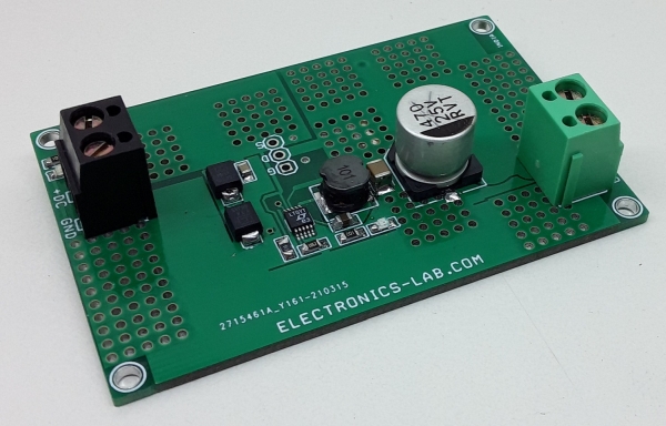
During fast SOURCE–DRAIN transients such as fast varying input (SOURCE) signals where the regulating 20mV loop is too slow, fast pull-up (FPU) and fast pull-down (FPD) current paths turn on and off the external MOSFET quickly. This rectifies the input signal the same way a diode would do but with much less power dissipation. The SOURCE and GATE pins are protected against reverse input voltages of up to –40V. GATE is pulled to SOURCE when SOURCE goes negative, turning off the MOSFET and isolating DRAIN from the negative input. The gate voltage for the external MOSFET is provided by the auxiliary boost regulator, which regulates its output AUX to 11V above DRAIN. D2 Input power LED, D4 output power LED, CN1 input , CN2 output.
WHAT IS ACTIVE RECTIFICATION?
Active rectification is a technique for improving the efficiency of rectification by replacing diodes with actively controlled switches like MOSFET-based circuits, whereas normal semiconductor diodes have a roughly fixed voltage drop of around 0.5-1 volts, active rectifiers behave as resistances, and can have an arbitrarily low voltage drop. Active rectification has many applications. It is frequently used for arrays of photovoltaic panels to avoid reverse current flow that can cause overheating with partial shading while giving minimum power loss. The constant voltage drop of a standard p-n junction diode is typically between 0.7 V and 1.7 V, causing significant power loss in the diode. Electric power depends on current and voltage: the power loss rises proportionally to both current and voltage.
Read more: ACTIVE RECTIFIER CONTROLLER WITH REVERSE PROTECTION FOR BATTERY AND SOLAR CELL
- What is the maximum load current this project supports?
The project is designed for a 5A load current. - How does the GATE amplifier regulate the forward voltage?
The GATE amplifier drives the MOSFET gate to maintain a constant 20mV drop across the device. - Can the circuit handle negative input voltages?
Yes, the SOURCE and GATE pins are protected against reverse input voltages of up to –40V. - Why is active rectification more efficient than using standard diodes?
Active rectifiers behave as resistances with arbitrarily low voltage drops, whereas standard diodes have a fixed drop of 0.5 to 1 volts causing significant power loss. - What happens during fast SOURCE–DRAIN transients?
Fast pull-up and fast pull-down current paths turn on and off the external MOSFET quickly to rectify the signal when the regulating loop is too slow. - How is the gate voltage for the external MOSFET generated?
An auxiliary boost regulator provides the gate voltage by regulating its output AUX to 11V above DRAIN. - What function do diodes D1 and D2 serve on the board?
They protect the IC from overvoltage spikes at the input. - What occurs if the voltage VDRAIN cannot support a 20mV drop?
The GATE amplifier drives the MOSFET off.