Summary of AT89C2051 DIGITAL SCALES CIRCUIT ATMEL
This article details the construction of a portable digital kitchen scale with a 2.5kg capacity and 10g accuracy. It utilizes strain gauges, an AD620 amplifier, and an AT89C2051 microcontroller to process weight data displayed on an LCD. The device features auto-power-off, low battery warnings, and an integrated Ni-Cd charger for portability.
Parts used in the Digital Kitchen Scale:
- AT89C2051 Microprocessor
- AD620 Instrument Amplifier
- TLC549 A/D Converter
- 4-Digit LCD Display (DIS1)
- Strain Gauge Sensor (DF2S-3/5kg)
- Ni-Cd Battery (ARK500/2)
- LM317T Voltage Regulator
- LM358 Operational Amplifiers
- BC5xx Transistor Series
- 24MHz Crystal Oscillator
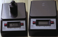
This is a kitchen scale with a maximum weight of 2.5kg and an accuracy of 10g. Exceeding the range is indicated by an acoustic signal and an LED. Weight is displayed on a four-digit LCD display. The weight also includes a weight-zero reset button. The power is solved by a battery whose discharge is below the set limit indicated by the LED.Then the battery needs to be recharged, otherwise the voltage drops below the operating level and the wrong weight information appears in the display. In order to avoid having to switch off the balance for unnecessary battery discharge, after 2 minutes of inactivity (only if there is no weight on the weight) it will turn itself off.
Block diagram :
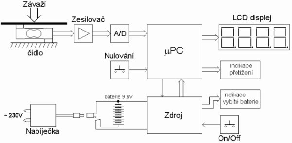
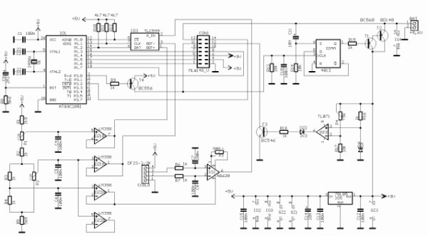
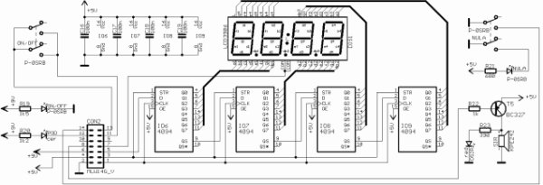
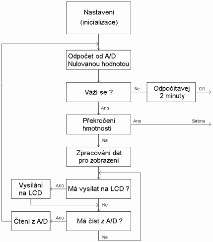
More detailed activity: Only IO4, transistor emitter T2, C11 and On / Off button are powered directly from the battery. Because the IO4 is made by CMOS technology, its take-off is minimal and hence the stand-by take-off of the whole balance when it is turned off. IO4 is connected as a T flip-flop (divider two). C11 and R14, after connecting the battery, sets output Q to log. H, the transistor T1 is closed, thereby interrupting the supply to the other part of the circuit. After pressing the button, CLK clock input is logged. H, the circuit is overturned, the transistors T1 and T2 are closed and the power balance of the rest of the balance is switched on. OZ3 is connected as a voltage comparator that monitors the battery voltage. If it drops below the set threshold by the trimmer P4, it switches on the transistor T3, which has an LED indicator in its collector and indicates a weak battery. For other circuits, we need a voltage + 5V, which is obtained from the IO5 stabilizer, C12 – C14 only serves to filter the voltage. The strain gauge sensing sensor is in the bridging circuit and at its output is a signal in the order of mV. This signal is too small for further processing, so integrated IC amplifier IO2 is connected to the circuit, its gain is 150 and is given by the Trimmer P3, which is set to 330. The amplified signal is further superimposed on the constant voltage (approximately 1 , 0 V), this is obtained from a multiple voltage divider and impedantly separated by the OZ2A operational amplifier. This amplified signal is applied to the A / D input IO3 converter. The range of the converter can be set by bringing two reference values to its REF + (about 2.7V) and REF- (about 1.1V) inputs. Both voltages are derived from the same voltage divider and impeded by OZ1. The size of the reference values can be set by the P1 and P2 trimmers to determine the lower and upper limits for the converter. According to the converter manufacturer, the difference between the reference values must always be greater than 1V. The amplified and converted signal is processed by the IO1 processor (more). The processor is in standard wiring, the C9 and R8 components ensure that when the processor reset is turned on, the Q1 crystal taps it at 24MHz.Output from the processor goes through the four 8-bit IO6-IO9 sliding registers that drive DIS1 segments on the LCD display. The common display terminal is connected directly to the processor port. Display segments need to be triggered by an AC signal with a frequency of 20 to 150 Hz (40 to 300x / s change). This means that the common outlet is set to the log. H and display the segments displayed in the log. L and vice versa the next time you broadcast. If the 2.5kg weight is exceeded (regardless of possible reset), the processor switches the transistor T5 and starts the piezo-siren SIR and the DSIR LED indicating overload. When the zero key is pressed, the processor port P3.2 is grounded, which is the input of the external interrupt and the processor remembers the current weight on the scale. If no weight is placed on the weight and is idle for 2 minutes, the transistor T4 switches on, which transmits the IO4 log to the CLK input. H, it flips and interrupts the power supply for the processor and other components except IO4. Weighing in operation is about 40mA.
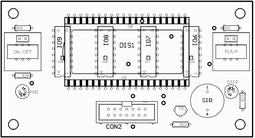
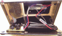
Bottom side – toolbar:
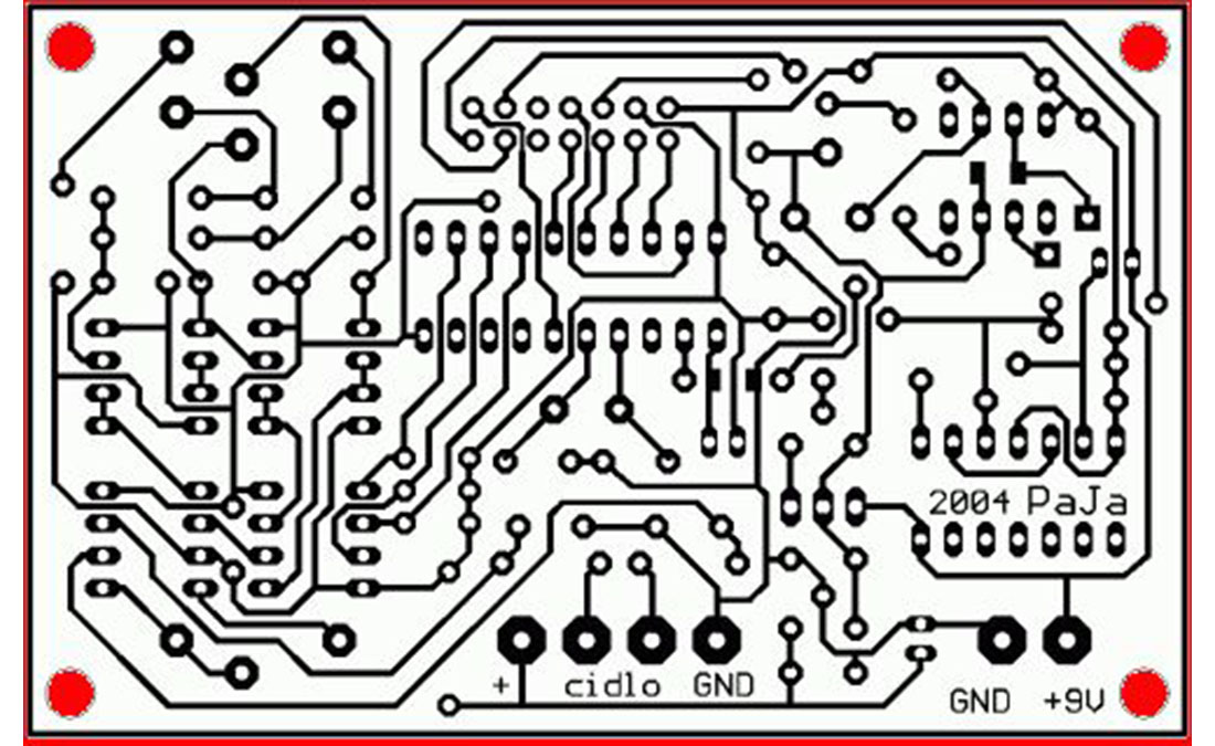
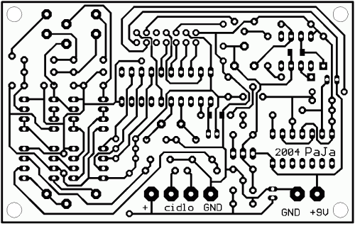
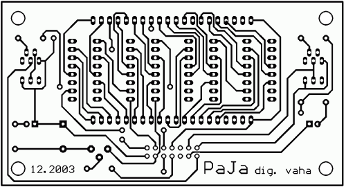
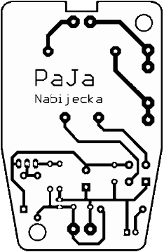
Design of printed circuit board (90 x 57 mm).
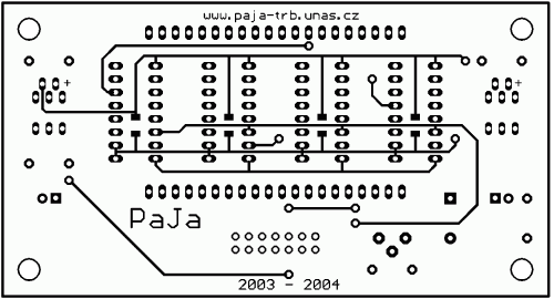
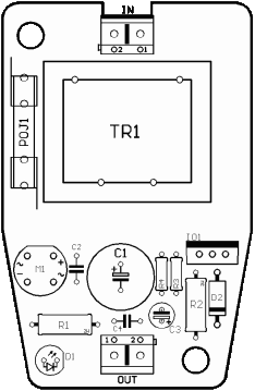
Design of printed circuit board (104 x 56 mm).
The program has about 300 lines and you can download it here – it’s complete with a lot of comments.
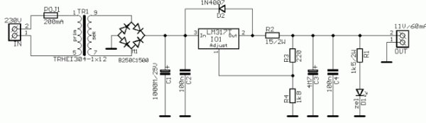
This is a simple charging connection for a Ni-Cd battery. This connection is not the most appropriate, but it is sufficient for occasional charging. I’ve chosen this simple connection to get the charger into the U-KPZ3 adapter box. The mains voltage is fed via a fuse to a transformer with a secondary voltage of 12V. This voltage is thrust across the M1 bridge, filtered through C1, C2 and applied to the LM317T regulated voltage stabilizer. With the R3 and R4 resistors the output voltage is set to 11.5V according to the formula U out = 1.25 (1 + R4 / R3). By R2, a constant charging current is set to 60 mA according to the formula I out = 1,25 / R2. This strain is filtered using C3, C4. The D1 LED serves only to indicate that the charger is on the network. The D2 protects the stabilizer against back-up by disabling the charger before disconnecting the rechargeable battery. It is advisable to place a small cooler on the IO1. The Ni-Cd battery is about to charge about 125% of the battery voltage, which in my case is 12V and current approximately 1/10 of the battery capacity, that is 60mA. I deliberately lowered the charging voltage to avoid potential battery damage.
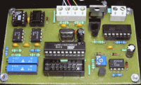
C1 100n C2, C3 22p - 2x C4-C8, C10, C12, C13, C15 - C19 100n - 13x C9 22M / 16V C11, C14 10M / 25V - 2x R1 1k8 R2 - R4, R6, R7, R9, R15, R18, R22 1k - 9x R16 1k SMD 1206 R5 560 R8 5k6 SMD 1206 R10 - R12 4k7 mini - 3x R13, R14, R17 10k - 3x R19 1k5 R20 1k2 R21 680 R23 390 P1, P2 PM19K001 - 2x P3 PM19E500 P4 PT-6VK005 DZ1 BZX83V056 DZ2 BZX83V033 T1 BC560 T2 BD140 T3 BC546 T4 BC556 T5 BC327 IO1 AT89C2051 IO2 AD620 IO3 TLC549 IO4 4013 IO5 78L05 IO6 - IO9 4094 - 4x OZ1, OZ2 LM358 - 2x OZ3 TL071 Q1 24MHz |
DIS1 LCD3906 DSIR LED 3mm red POD LED 3mm red Strain gauge DF2S-3 / 5kg ZERO, ON / OFF P-0SRB - 2x SIR KPE242 BAT ARK500 / 2 CIDLO ARK500 / 2 - 2x CON1, CON2 MLW14G - 2x PFL14 connectors - 2x flat cable AWG28-14 (15cm) B-8F600AA battery power connector K3716A display frame AR1950 Charger : C1 1000M / 25V C2, C4 100n - 2x C3 4M7 / 50V R1 1k5 / 2W R2 15 / 2W R3 220 R4 1k8 D1 LED 3mm green D2 1N4007 IO1 LM317T M1 B250C1500 TR1 TRHEI304-1x12 IN, OUT ARK500 / 2 - 2x POJ1 KS20-01 footrest tube fuse 200mA adapter box U-KZ3 power connector SCP-2009B cable to connect the charger to the balance |
Source: http://paja-trb.unas.cz/elektronika/konstrukce/vaha.html Digital Scales project Alternative link:at89c2051-digital-scales-circuit-atmel.RAR
- How does the scale indicate if the weight limit is exceeded?
An acoustic signal from a piezo-siren sounds and an LED lights up when the 2.5kg limit is surpassed. - Can the scale be reset while a container is on it?
Yes, pressing the zero button allows the user to tare the weight so only the added contents are measured. - What happens if the battery voltage drops below the operating level?
The display will show incorrect weight information unless the battery is recharged immediately. - Does the scale turn off automatically?
Yes, the balance switches itself off after 2 minutes of inactivity provided no weight is placed on the platform. - How is the small sensor signal amplified?
The output voltage from the strain gauge bridge is amplified by a factor of 150 using the AD620 instrument amplifier. - What component processes the digital value into a readable weight?
The AT89C2051 microprocessor converts the A/D converter values into the correct weight reading for the display. - Is there a specific charging current for the battery?
The charger is set to provide a constant charging current of approximately 60 mA. - How does the low battery indicator function?
A comparator circuit monitors the voltage and switches on a transistor to light an LED indicator when the threshold is crossed.