Summary of Dual Trace Oscilloscope
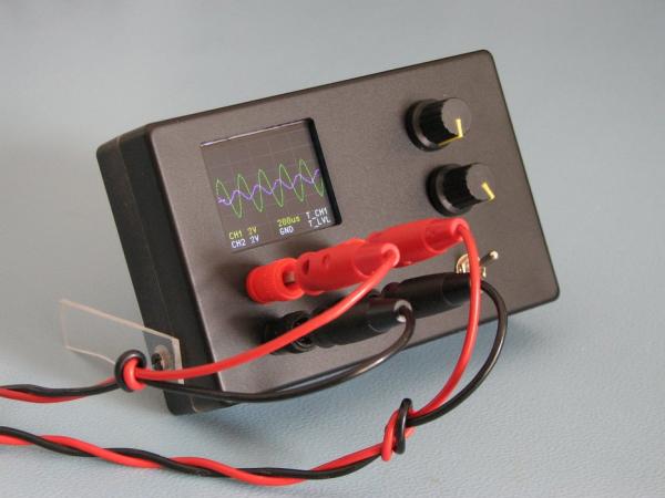
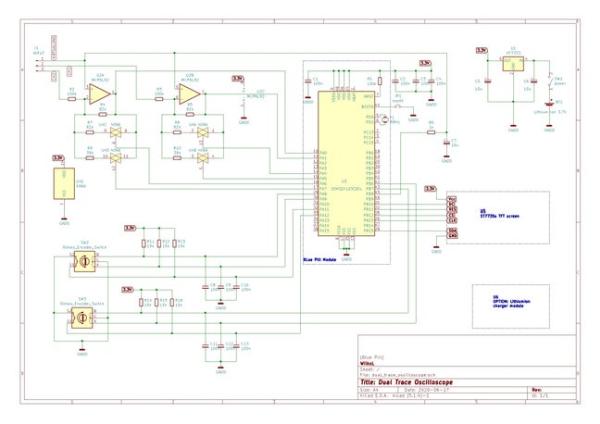
This article details the construction of a dual-trace oscilloscope using a Blue Pill STM32F103 microcontroller. The project aims to provide two input channels with variable sensitivity and triggering, surpassing a previous single-channel mini-oscilloscope. Key design challenges included managing analog switches for attenuation, creating a virtual ground for single-supply operation, and implementing software debouncing for rotary encoders. The author utilized DMA and overclocked ADCs to achieve sampling speeds up to 1.6 MSamples per second, displaying waveforms on an ST7735s TFT screen within a compact plastic enclosure.
Parts used in the Dual Trace Oscilloscope:
- plastic box
- perfboard (double sided prototype board 8x12cm)
- Blue Pill
- ST7735s TFT display
- lithium-ion battery
- HT7333 3.3V low dropout regulator
- MCP6L92 dual opamp
- TSSOP8 to DIP8 board
- 12 MHz crystal
- rotary encoder plus knob (2x)
- powerswitch
- banana terminals (4x)
- lithium-ion charger board
- several resistors and capacitors
- nylon spacers, nuts and screws
When I build my previous mini oscilloscope I wanted to see how well I could make my smallest ARM microcontroller a STM32F030 (F030) perform, and it did a nice job.
In one of the comments it was suggested that a “Blue Pill” with a STM32F103 (F103) might be better, smaller than the development board with the F030 and possibly even cheaper. But for the mini oscilloscope I did not use the development board but the F030 on an even smaller SMD-DIP board, so there a Blue Pill would certainly not be any smaller and I doubt that it would be cheaper too.
Code is now available on Gitlab:
https://gitlab.com/WilkoL/dual-trace-oscilloscope
Supplies:
Part list:
– plastic box – perfboard (double sided prototype board 8x12cm) – Blue Pill – ST7735s TFT display – lithium-ion battery – HT7333 3.3V low dropout regulator – MCP6L92 dual opamp – TSSOP8 to DIP8 board – 12 MHz crystal (not necessary) – rotary encoder plus knob (2x) – powerswitch – banana terminals (4x) – lithium-ion charger board – several resistors and capacitors – nylon spacers, nuts and screws
Tools:
– soldering station – solder 0.7mm – some wire – side cutter – glasses and loupe – drill – multimeter – oscilloscope – STLink-V2
Software:
– STM32IDE – STM32CubeMX – STLink Utility – LowLayer library – adapted library for ST7735s – Notepad++ – Kicad
Step 1: Interleave or SImultaneous Mode
Blue Pill
But the idea was there, and I knew that the F103 has two ADCs! What if I used those two ADCs together in “interleave” mode, something I have done before with the STM32F407 (F407). The sampling speed would double. That, combine that with a faster microcontroller and it would make for a great successor to the mini oscilloscope.
Interleave mode
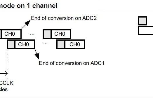
Oddly the ADCs in the F103 are less advanced than the one in the F030 (and the F407), you cannot choose the resolution. More important is that you also cannot change the timing between the two ADCs. Now, when you use the interleave mode usually you want the sampling as fast as possible with the shortest time between any samples, but with an oscilloscope it is neccessary to change the timing. Maybe it still can be done, I’m not a professional oscilloscope designer, but I dropped the plan to use interleave-mode.
Simultaneous mode
But, having two ADCs gives many more options, the two ADCs can be set to “regular-simultaneous” mode too. How about a dual trace-oscilloscope?
Having decided to try to make a dual trace oscilloscope I also wanted to have variable input sensitivity, an option that I did not have on the mini oscilloscope. That means an attenuator (and amplifier) on the inputs. And maybe I wanted even more? So I made a small list of “nice-to-haves”.
WISH LIST
two channels
variable sensitivity on both channels
triggering on both channels
variable trigger level on both channels
variable offset
single battery power
fit in the same box as the mini-oscilloscope
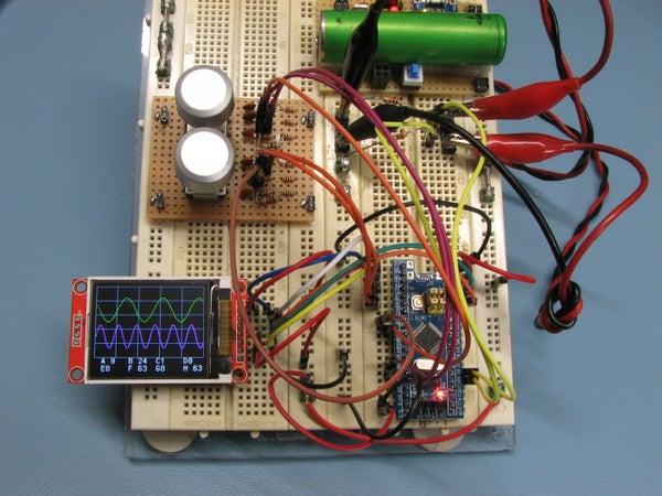
Step 2: Prototyping
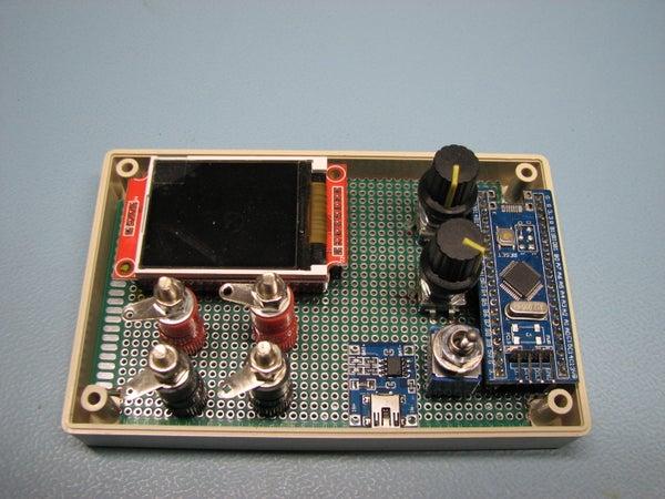
As usual I started this projects on a breadboard. (See picture) And before soldering everything on the perfboard I try to find out if and how it will fit in the chosen project box. It fits, but only just. Some parts are hidden under the screen, other under the Blue Pill. And again, just as for most of my projects, this is a once-only project and I will not design a PCB for it.
Step 3: Attenuators
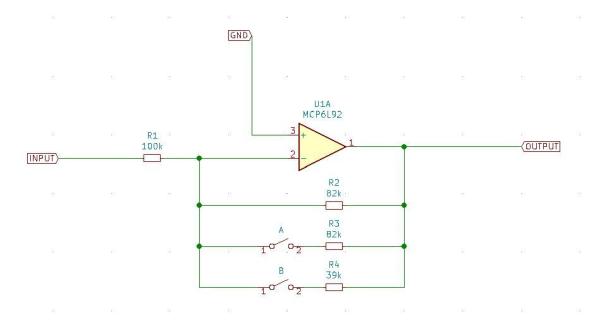
In regular oscilloscopes the input attenuators are circuits that change attenuation and amplification by switching in and out resistors with small signal relays. While I have some of those relays, I know they will not switch at less than 4 Volt, that means that they will only work with a fully loaded Lithium Ion battery (4.2V). So I needed another way to switch those resistors. Of course I could just install mechanical switches, but that would certainly no longer fit in the project box in had in mind, perhaps I could try a better digital potentiometer again (the one I have is way too noisy).
Then I thought of “analog switches”, with those I can make a digital potentiometer myself. In my parts collection I found the CD4066 with four analog switches. The idea is to make the feedback resistor of an opamp variable by switching in and out resistors parallel to the feedback resistor.
It works very well, but having just 4 switches in the 4066 and having 2 channels it was not possible to make more than three sensitivity levels. I chose 500mV, 1V and 2V per division as those are the voltage levels that I use most. The screen is divided into 6 divisions, so that makes for the ranges -1.5V to +1.5V, -3V to +3V and -6V to 6V.
With the “virtual-ground” you can move these ranges up and down so even 0v to +12V is possible.
Step 4: Virtual Ground
Because the oscilloscope uses a single power rail (3.3V) the opamps need a virtual ground level or they will not work. This virtual ground level is made with PWM on one output channel of TIM4, the duty cycle of it changes from just a few percent to almost a hundred percent. A low pass filter with a 1k resistor and a 10uF capacitor transforms that into a voltage of (almost) 0V to (almost) 3.3V. The frequency of the squarewave is just under 100kHz, so the simple low pass filter is good enough.
Rather late in the building of this oscilloscope I realized that you cannot have two separate offsets for the channels. This is because of the fact that with a single power supply the input-ground-level has to be separate from the real ground level of the opamps. So both channels move in the same way as you change the GND-setting.
Step 5: Rotary Encoders and Debugging
On the mini oscilloscope I used just one rotary encoder for all functions. That would make a dual oscilloscope very difficult to use, so here I need two. One encoder for the attenuators and virtual ground level and the other encoder for the timebase and triggering. Sadly, just as in my other project, these rotary encoders are very “noisy”. They are so bad that they simply would not work with timers in “encoder-mode”, the standard way of reading them. I had to make a debouncing mechanism with timer TIM2, checking the encoders every 100us. This timer in turn is started (only) when there is some activity on the encoders, this is checked with the EXTI functionality on the input ports. Now the encoders work well.
And as you can see, having a display can also be very handy to display debugging information.
Step 6: Display and Timebase
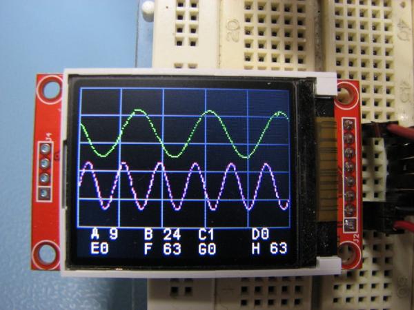
The display has a resolution of 160 x 128 pixels so there are 160 samples needed for one screenfull, I managed to speed up the ADCs to do 1.6 million samples per second and that, with the much overclocked microcontroller (more on that later), gives a minimum timebase of 20us per division (100us per screen). Thus a waveform of 10kHz will fill the whole screen.
That is only twice as fast a the mini oscilloscope I made before. Oh well, now it is with two channels :-).
As said, the display is 160 pixels wide so only 160 values are needed per screen. But all buffers actually contain 320 samples. So the DMA stores 320 values before it triggers a transmission complete interrupt (TC). This is because the triggering is done in software. The sampling starts at a random moment, so it is very unlikely that the first value in the buffer is the place where the trigger point should be.
Therefore the trigger point is found by reading through the trace_x_buffer, if the value is at the wanted trigger value en if the previous value is just below it, the trigger_point is found. This works quite well, but you need a bigger buffer than the actual display size is.
This too is the reason that the refresh rate on the lower timebase settings is slower than you might expect. When you use the 200ms/div setting one screen full of data is 1 second, but because double the amount of conversions is done, that takes 2 seconds. On the faster timebase settings you will not notice it that much.
TIM3 is used to generate the timebase. It triggers the ADCs with the speed as required by the selected timebase setting. Its clock of TIM3 is 120MHz (see OVERCLOCKING), the maximum number to which it counts (ARR) determines how other it overflows or, in ST language it updates. Via TRGO these update pulses trigger the ADCs. The lowest frequency it generates is 160 Hz, the highest is 1.6MHz.
Step 7: ADCs and DMA
The two ADCs convert the voltage on their inputs at the same time, they store those two 12 bit values in a single 32bit variable. So the DMA has just one variable per (double) conversion to transfer.
To use these values it is therefore necessary to split them into the two values so they can be used to display the two traces. As said, ADCs in the F103 cannot be set to other resolutions than 12 bits. They are always in 12 bit mode and so conversions always take the same number of clock pulses. Still, with the overclocking of the ADCs , 1.6 MSamples per second can be done (see Extra: Overclocking).
The reference of the ADCs is Vdd, the 3.3V rail. To convert that to more convenient values (per division) I have calculated the values of the attenuators, because I do not have the exact resistor values that come out of those calculations some corrections are done in software.
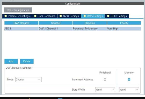
In this project I use DMA in “regular-mode”. In this mode the DMA stops transferring data (from de ADCs to memory) when the number of words (or half-words or bytes) all are transferred. In the other possible mode, “circular mode” the DMA resets itself and continues transferring data un-interrupted. That did not work with the F103, it is so fast that it overwrites the data in the adc_buffer[] before the rest of the program could read it. So now the process is as follows:
– setup DMA to the number of data to be transferred and enable DMA
– start the triggering of the ADCs, these will request DMA transfers after each (double) conversion
– after the set number of conversions are transfered, DMA stops
– immediately also stop triggering of the ADCs
– do all manipulation needed on the data in memory
– show traces on the screen
– start the process again
Source: Dual Trace Oscilloscope
- Why was the interleave mode plan dropped?
The plan was dropped because the F103 ADCs cannot change timing between the two converters, which is necessary for an oscilloscope. - How are input attenuators implemented without relays?
Analog switches from a CD4066 chip are used to switch resistors in parallel with the opamp feedback resistor. - What voltage levels were chosen for the sensitivity ranges?
The chosen levels are 500mV, 1V, and 2V per division. - How is the virtual ground created for the single power supply?
A PWM output from TIM4 drives a low pass filter made of a 1k resistor and a 10uF capacitor. - Why were two separate rotary encoders required?
One encoder controls attenuators and offset while the other controls timebase and triggering, making the dual scope easier to use. - How does the system handle software triggering?
The buffer stores 320 samples even though only 160 are displayed, allowing the code to search for the specific trigger point after sampling stops. - Why is the refresh rate slower on lower timebase settings?
Doubling conversions for two channels means it takes longer to fill the buffer; for example, 1 second of data takes 2 seconds to acquire. - What resolution do the ADCs operate at?
The F103 ADCs are fixed at 12-bit resolution and cannot be changed.