Summary of OnChip Establishes New Capability to Provide Hi-Rel Visual Inspection Services for Wafers or Bare Die Semiconductors
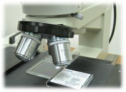
OnChip has launched a visual inspection service for semiconductor ICs, utilizing low and high-power microscopes to detect defects like foreign material, voids, contamination, scratches, and dicing issues. This process adheres to Commercial, Military, and Medical Electronics specifications, often following MIL-STD-883 Method 2010. The service is performed by experienced staff on either wafers or diced chips in trays such as waffle packs or gelpaks, ensuring device reliability through rigorous defect removal.
Parts used in the OnChip Visual Inspection Project:
- Low power microscopes
- High power microscopes
- Wafers
- Sawn devices
- Waffle packs
- Gelpaks
Santa Clara, CA (PRWEB) January 22, 2012
OnChip has established new capability to offer 100% visual inspection using both low and high power microscopes that meet Commercial, Military and Medical Electronics specifications. Inspection is done to look for various types of visual defects.
Some of the more common defects include:
Embedded foreign material
Metallization or Passivation voids & irregularities
Contamination such as liquid or adhesive residues and surface particles
Surface scratches caused by test probes or wafer handlers
Dicing defects such as chip outs and cracks
Semiconductor ICs (Integrated Circuits) are extremely fragile and endure a variety of stresses during wafer fabrication, testing and dicing. They are easily prone to defects that would either prevent the device from operating correctly or pose a reliability concern for long-term operation. These defects are caused either during wafer fabrication or mechanically-induced during handling. The extent to which any defect may be acceptable would be defined by the appropriate criteria selected to fit the application environment. Units that are defective can be effectively removed by visually inspecting the devices under high magnification. There are many different inspection criteria, but the most common one is MIL-STD-883, Method 2010. This inspection standard defines the equipment to be used for the inspection, magnification ranges, what defects to look for and quantifies the amount of any particular defect that is acceptable.
The ability to visually inspect a circuit requires a lot of skill and training, which increases through experience and a continuous training program. OnChip employs a highly qualified staff of inspectors who have over 30 years of experience in this field. The company works very closely with customers during the initial phase to ensure proper calibration to the inspection needs. Visual inspection services are offered either in wafer-form or after the device has been sawn and placed in chip trays such as waffle packs or gelpaks.
###
- What types of defects does OnChip inspect for?
Defects include embedded foreign material, metallization voids, contamination, surface scratches, and dicing defects like chip outs. - Can the inspection meet military electronics specifications?
Yes, the microscopes used meet Commercial, Military, and Medical Electronics specifications. - Which standard defines the most common inspection criteria?
The most common standard is MIL-STD-883, Method 2010. - How are defective units removed during the process?
Defective units are effectively removed by visually inspecting the devices under high magnification. - Does the inspection require specific training?
Yes, the ability to visually inspect requires skill, training, and experience. - In what forms can the visual inspection services be offered?
Services are offered in wafer-form or after the device has been sawn and placed in chip trays. - What kind of chip trays are mentioned for holding devices?
The article mentions waffle packs and gelpaks as types of chip trays used.