Summary of PCB Via Design: What is it and what are the types?
Vias are plated holes that connect PCB layers; types include through-hole, blind, buried, microvias, and various protection/filling techniques. Blind/buried and microvias enable high-density interconnects but add manufacturing complexity and cost. IPC-4761 defines protection methods like tenting, open vias, solder mask plugging, and filled/capped vias (non-conductive or conductive). Designers should use EDA tools to export separate drill files and verify Gerbers (e.g., HQDFM) for DFM issues. HQ NextPCB offers many via types and filling options with instant quoting for cost and lead-time.
Parts used in thePCB Via Types and Protection Project:
- PCB substrate (multilayer board)
- Copper plating for via barrels
- Drill bits (mechanical and laser)
- Prepreg and core materials for stack-up
- Solder mask
- Non-conductive epoxy/resin (via fill)
- Conductive epoxy/resin (via fill)
- Electroplating equipment
- Via plugging/capping materials and processes
- Gerber and drill file exports from EDA software
- HQDFM Gerber viewer / DFM analysis tool
Vias have become crucial components of double-sided printed circuit boards (PCBs). As PCB fabrication technology has advanced and the demand for small yet powerful electronics has grown, the variety of via sizes and types has expanded. In this article, we aim to cover every type of via, including when to use them in your PCB design, how they appear in PCB manufacturing files or Gerber files, and their impact on production costs.
PCB vias are small holes plated with copper that transmit electrical signals from one conductive layer to another. These vias are typically created by drilling holes in the PCB substrate during the early stages of production. The walls of the holes are then plated to form the vias.
The main difference between vias and through-holes lies in their purpose. Vias are used for conducting signals between layers, while plated through-holes (PTHs) are necessary for soldering through-hole components to the boards and connecting them to the circuitry. The plating process slightly reduces the hole diameter, so PCB CAM engineers use larger drill bits to compensate and ensure the desired hole sizes in the Gerber and drill files. Vias with a diameter smaller than 0.5mm are typically considered vias, although it can be challenging to determine with smaller components.
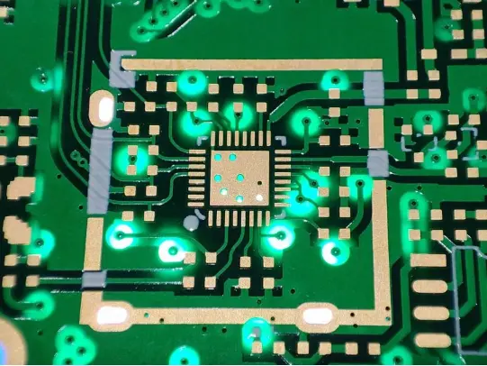
Through-hole vias are standard vias that go through the entire board, connecting all layers with a via “barrel.” In exported Gerber files, vias are represented by filled pads on connected copper layers with a centered drill hole. In inner layers where no electrical connection to the via is needed, PCB EDA software adds antipads, which are clearances from the via drill or annular ring to the plane.
Almost every PCB design nowadays includes plated holes in some form, making hole plating a standard part of the production process. Additional costs for vias are usually not a concern unless tiny vias are used or there are a large number of vias on a single board.
Blind and buried vias are named based on their visibility on the PCB board. Blind vias are only visible on one side of the board, while buried vias are not visible from the outside at all. These vias are drilled at different stages of production and filled or plugged to ensure planarity. The term “through-hole via” for regular vias becomes apparent when compared to blind/buried vias, as regular vias go entirely through the boards. Blind/buried vias are typically used in high-density designs where there is limited space for regular vias. Designing high-density interconnects (HDI) with blind/buried vias can be complex and may require additional lamination and plating cycles.
When designing with blind/buried vias, it is important to consider the manufacturing complexity associated with them. Some combinations of blind/buried vias may not be possible or can significantly increase production costs. Custom board stack-ups, prepreg thicknesses, aspect ratios, microvias, and via filling/plugging all play a role in blind/buried via design. Designers should conduct thorough research and explore alternative options if feasible.
To request blind/buried vias, designers should use EDA software with these capabilities to export separate drill files for through, blind, and buried vias. The files should be appropriately labeled to indicate which layers the vias connect.
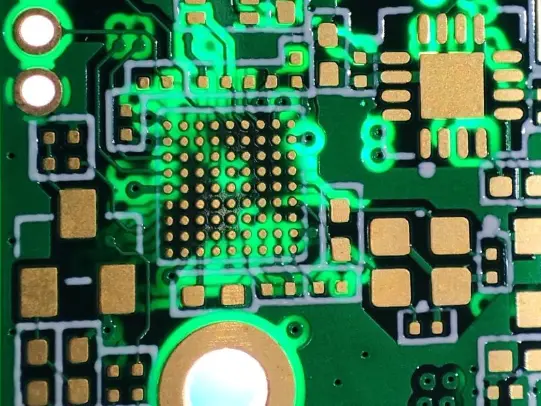
Microvias, as the name suggests, are smaller than regular vias and have a 1:1 diameter to depth ratio relative to the board thickness. They can be created through laser drilling, but this method is limited to very small thicknesses. Microvias can be used as blind vias in HDI designs to maximize board space. However, microvias require specialized laser drilling equipment and via filling machines, making them advanced capabilities that may not be available in all PCB factories. Therefore, microvias should only be used when absolutely necessary.
By using only microvias (blind vias), the manufacturing complexity can be slightly reduced by eliminating the extra lamination step required for blind vias. Without blind vias, production only requires one lamination and plating step, similar to regular multi-layer boards.
Via Protection Types According to IPC-4761
IPC-4761, the Design Guide for Protection of Printed Board Via Structures, outlines seven different via protection types or techniques for PCBs. Each type has its own uses and can vary significantly in cost. Selecting the appropriate via protection type is an important part of a designer’s strategy for reducing board defects and increasing the reliability of the boards within the available budget.
- Tented vias: This is the most common method of via protection. During fabrication, the solder mask is applied according to the Gerber file, covering the vias. However, larger holes may not be fully covered, which can lead to debris entering the via and causing corrosion and reliability issues. Tented vias can also burst open when exposed to high temperatures.
- Opened (uncovered) vias: In this method, the via pads are exposed and treated with surface finish, similar to other exposed copper elements. Opening vias is often done for testing purposes, but it leaves them vulnerable to corrosion and accidental solder bridges.
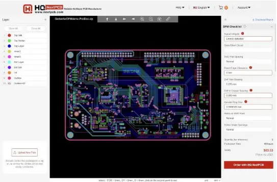
In certain situations, designers may be unaware that their vias are open. While PCB design software should have settings to specify whether vias should be open or tented, the only way to ensure accuracy is by checking the Gerber files. This is where a Gerber viewer like HQ NextPCB’s free online Gerber viewer, HQDFM, can be helpful.
With HQDFM, designers not only have the opportunity to review the actual instructions they are sending to PCB manufacturers, but they can also analyze over 20 potential Design for Manufacturing (DFM) issues that may impact production or affect the performance of the boards. By simply clicking a button, HQDFM generates a detailed report highlighting each problem and provides suggestions on how to resolve them.
- Via Filling/Plugging: This technique involves filling the vias with various materials, including solder mask, non-conductive epoxy/resin, or conductive epoxy/resin. Plugging refers to partially blocking the via barrel, while filling means completely filling the via barrel with no gaps. Capping involves plating the top vias with a solderable pad.
- Solder Mask Plugging (and tenting): Technicians push solder mask into the vias using an aluminum squeegee, followed by covering them with solder mask as in tented vias. This method guarantees that the vias are plugged with solder mask, but it may not eliminate gaps and air pockets.
- Filled and Capped Vias: In this technique, the vias are filled with either non-conductive or conductive resin. The surface is then ground flat and cleaned, followed by a separate electroplating step to create planar pads on top of the vias. Non-conductive resin fill is commonly used
Non-conductive resin/epoxy is commonly used to fill vias on surface mount pads to prevent solder from wicking away and causing soldering defects and board reliability issues. These vias, known as via-in-pads, are necessary for high-density designs and small BGA footprints. They can also be helpful in reducing parasitic inductance and capacitance effects.
On the other hand, conductive epoxy is sparingly used to increase the thermal conductivity of vias. However, it is not commonly chosen due to the high cost of processing and the availability of cheaper and more effective methods for heat dissipation.
It’s important to note that filling vias with non-conductive resin does not affect their electrical conductivity or signal strength. The via barrel remains intact, ensuring the same signal transmission as regular vias.
HQ NextPCB offers a wide range of PCB via types, including through, blind, and buried vias, microvias, and various protection techniques such as open, tented, solder mask plugged, and tented vias. They also provide via filling with non-conductive resin. By using their instant quotation platform, you can easily add these via types and techniques to your board and see the price and lead time upfront.
As a specialized manufacturer of high-reliability multilayer boards, HQ NextPCB ensures that your board’s vias will withstand the test of time. Get an instant quotation from HQ NextPCB now to experience their reliable services.
- What is a via in PCB design?
A via is a small plated hole that transmits electrical signals between conductive layers of a PCB. - How do through-hole vias appear in Gerber files?
They appear as filled pads on connected copper layers with a centered drill hole and antipads on inner layers where no connection is needed. - When should blind or buried vias be used?
They are used in high-density designs where limited space prevents using regular through-hole vias. - How are microvias created and when are they used?
Microvias are often laser drilled, used as blind vias in HDI designs, and are chosen when small size is necessary. - What are common via protection types per IPC-4761?
Common types include tented vias, opened (uncovered) vias, solder mask plugging, and filled and capped vias. - Does filling a via with non-conductive resin affect signal transmission?
No; filling with non-conductive resin does not affect electrical conductivity because the via barrel remains intact. - Why might conductive epoxy filling be rarely used?
Because it is costly and often less effective compared to cheaper methods for heat dissipation. - How can designers ensure vias are tented or opened as intended?
By checking exported Gerber files with a viewer like HQDFM and ensuring EDA software settings specify via tenting or opening. - What manufacturing complexities do blind and buried vias introduce?
They can require additional lamination and plating cycles, custom stack-ups, specific prepreg thicknesses, and via filling/plugging processes. - Can using only microvias reduce manufacturing steps?
Yes; using only microvias as blind vias can eliminate an extra lamination step, requiring only one lamination and plating like regular multilayer boards.