Summary of Phased Array Speaker System
For our ECE 4760 final project we built a 12-element acoustic phased-array: the system samples standard audio at ~44.1 kHz, applies independently adjustable time delays per channel via an ATmega644, and outputs through DACs, filters, and speaker drivers to steer the beam direction across frequencies. Simulations validated wideband steering via pure time delay. Key challenges included ISR timing, ADC/DAC selection, thermal management, and mechanical assembly on scavenged power and fan hardware.
Parts used in the Phased Array Speaker System:
- 12 low-cost speakers
- ATmega644 microcontroller (20 MHz crystal)
- TLC0831 ADC
- Two Maxim MX7228 octal 8-bit parallel DACs
- LF353P op amp (input amplifier)
- LM324N quad op amp (Sallen-Key low-pass filters)
- NPN transistor for current reference
- N-channel MOSFETs for current mirror
- Resistors and capacitors for filters and bias networks (various values specified in text)
- 680 μF series coupling capacitors for speakers
- Aluminum box-beams, plywood, screws, stand-offs, hot glue for mechanical assembly
- Computer ATX power supply (scavenged) providing ± and 12V rails
- 12V cooling fans (scavenged)
- Potentiometer for user interface
- External crystal (20 MHz)
- Decoupling capacitors
- Wiring, headers, and connectors
Introduction
For our ECE 4760 final project, we designed and built an array of 12 independently-controllable speakers to implement an acoustic phased-array system. The system samples a standard audio input signal at approximately 44.1 kHz, and then outputs this signal to each of 12 speakers, each with a variable delay. The idea behind a phased-array is that by changing how the speakers are driven the angle of the maximum intensity of the output wave can be shifted. This will be further explored in the high level design of the project. This type of array was built to be able to support various other more advanced design challenges, including longer-range acoustic modem transmission and sonar imaging.
High Level Design
Rationale
The initial rationale behind this project was our desire to build a sound system that can direct or shape sound into a specific shape. We knew about phased-arrays for use in microwave and EM applications, and knew the math was the same for acoustic waves. Furthermore, we found that building a wide-band phased array required true time delay between the elements, a task that a microcontroller is particularly well-suited for. The mathematical modeling we did showed that we would be able to steer sound intensity effectively given the size and complexity of an array we could build. Furthermore, all commercially-available speaker phased-arrays are prohibitively expensive – the least expensive we found was over $2000. These facts all inspired us to implement our own affordable speaker array.
Background Math
The physics of a phased-array of transmitters can be derived from the math for a diffraction grating. A diffraction grating assumes N sources of aperture a spaced distance d apart transmitting at a wavelength λλ. Below is an example of such a system (in this case, the system we built).
In the far-field, the wave function of such a system is
When we add a phase term, ϕϕ, to the second part of the equation, it becomes
Next, we square the wave function to get what we are interested in, intensity of the wave.
Since the second term is the only term dependent on the phase of the elements, we can estimate the maximum angle by setting the numerator of the second term to its maximum value, 1, and solving for θθ in terms of ϕϕ.
Assuming N is significantly larger than ππ, we can see that the first term becomes negligible and
Thus, we can see that we should expect the angle of maximum amplitude to be a function of both the phase shift of the wave, and its wavelength (assuming the distance between the sources is fixed). For microcontroller coding, we would prefer to not require different calculations for each frequency. Fortunately, some mathematical manipulation shows us an easier method of adjusting the angle for all frequencies at once.
First, we make the substitution based a fundamental wave equation relating wavelength, frequency, and the velocity of sound.
We then recognize that for any frequency, ϕfϕf is equivalent to a time delay. Thus we get
Now we have an equation that relates the maximum power angle to delay time between the elements. This equation has no dependence on wavelength, indicating it should hold true for a large band of frequencies. Since many approximations were made throughout this derivation, we did significant simulation in MATLAB to show the principles found here apply.
MATLAB Simulation
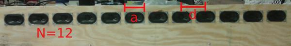
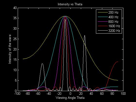
The intensity equation was implemented in MATLAB to determine the wave intensity output of the speaker array with respect to the viewing angle. The adjustable parameters are the number of elements N, the distance between adjacent speakers d, the width of the speakers a, the wavelength of the sound wave λλ, and the time delay between signals going to adjacent speakers. Once the mechanical set up of the speaker system was finished the only parameters that were free to change were the wavelength and time delay. The number of speakers was 12, the distance between adjacent speakers was 0.085m, and the width of the speakers was 0.07m.
Using the simulation we were able to show that the main lobe for different frequencies could be adjusted with a time delay. This is important because if different frequencies would not be shifted evenly for a given time delay then a more complicated solution would have to be implemented, such as taking the FFT (Fast Fourier Transform) of the input signal, adjusting the phase terms in the frequency domain, and then returning to the time domain using the IFFT (Inverse Fast Fourier Transform). The problem with this solution is that the microcontroller would not be able to perform the calculations before it was time to play the next data sample. The simulation also showed that a time delay would shift the beam in only one direction. For the beam to be steered to the other side a negative time delay is necessary, which corresponds to changing which end speaker is defined as the lead speaker. The following plots show steering multiple frequencies by changing the time delay. The first plot shows no time delay, and the maximum intensity of all frequencies are centered at 0 degrees.
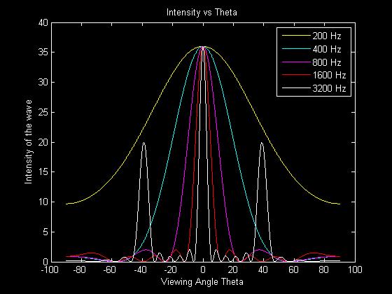
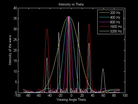
The next two plots show time delay differences between the outputs of +.3ms and -.3ms respectively. As the graphs show, all the frequencies are shifted by the same angular amount, having their maximum at the same angle.
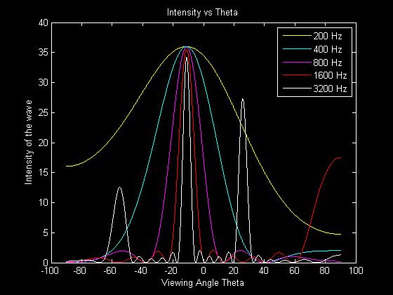
Thus, we have shown through simulation that wide-band beams can be steered through pure time delay, and no more advanced phase shifting is necessary.
Logical Structure
(Note: more detail on all the hardware and software discussed in this section can be found in the design section of this site)
The overall structure of our hardware design is illustrated in the flow-chart below:
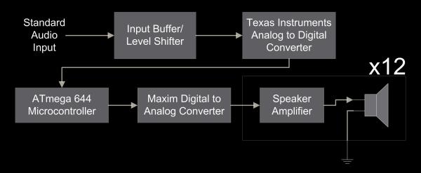
Our input is taken from any standard audio source. Inspection of multiple audio outputs with an oscilloscope confirmed that standard output is generally a signal varying between plus and minus 1V. To get the full use of our Analog to Digital converter (ADC), we needed a signal that varies between 0 and 5V. Therefore, we used an input amplifier to re-bias and amplify the signal before going into the ADC. The ADC then communicates the digital value of this input signal to the ATmega microcontroller. The microcontroller performs the necessary mathematics for the desired phase shift between the speakers, and then outputs each channel to a Digital to Analog converter (DAC). This output is then passed to a speaker amplifier, which both applies a low-pass filter to the signal and buffers it before outputting it to the speaker. The low-pass filter is necessary because the use of DACs introduces quantization noise which we wanted to remove, and the buffer is necessary because the impedance of the speaker is only 8 ohms, much lower than the output impedance of the DAC.
The overall structure of our software design is illustrated below:
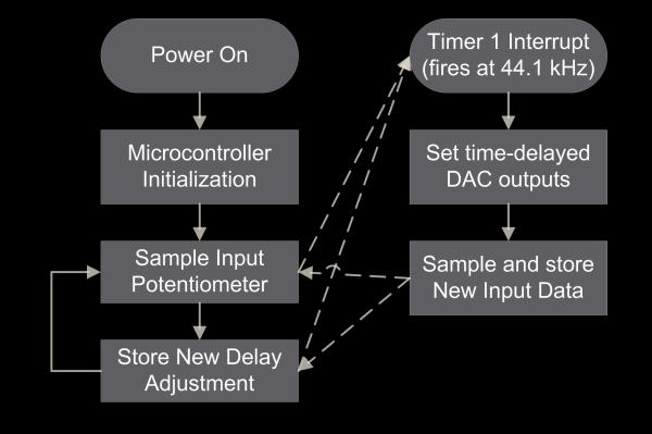
Upon power-up the microcontroller initializes its hardware. This includes setting up SPI communication with the ADC, setting up the internal ADC, and setting up the timer interrupts to ensure we get sound capture and play-back at a well-defined frequency. Once this hardware is initialized, the main loop of the program runs. This is fairly simple, it reads an input channel connected to a potentiometer which acts as the user interface, and then sets the delay for the desired angle accordingly. This main loop is interrupted at a frequency of 44.1 kHz to perform audio capture and playback. In the interrupt, the time-delayed outputs are sent to each channel of the DACs, and the new input data is sampled from the ADC. This code seems rather simplistic, but the biggest challenges came in the implementation details – specifically it was challenging to both get this code to run at 44.1kHz and to have it fit in the RAM effectively. These challenges will be discussed in the software design section.
Design Trade-offs
We had to make a few design trade-offs in hardware, most of which were budget-related. First, we had to trade-off between the number of speakers we used, and the quality of the audio produced by the speakers. Due to our budget constraints, higher-quality speakers with more advanced amplifier circuits would necessarily mean we had to use fewer speakers. We settled on using 12 speakers, which according to our simulation would give us relatively good frequency control in our desired range, while still being affordable. We also chose very low-priced speakers which necessarily hurt our sound quality, but we were mostly interested in this project being a proof-of-concept, and we knew we would get more effective results with more speakers in a larger array.
Another hardware design trade-off we made was in our selection of power-supply. We chose to use a computer power supply that we scavenged since it gave us the power we needed at the necessary voltage, and didn’t count against our budget. The trade-off here is that the rails from the computer power supply are slightly noisier than those from an isolating power supply, and some of that noise came through on the speakers. Again, we were more interested in having a large array to prove our concept worked than having perfect sound quality, so budget-wise it made most sense to use the computer power-supply.
A more physical trade-off we had to consider was adjusting the distance between our speakers versus the size of the whole array. Our simulation showed that using a larger array gives us better control over lower frequencies, while using elements spaced more closely together gave us better control over higher frequencies. Since we could only fit 12 speakers into our budget, these two variables were at odds with each-other. We decided on a spacing of .5 inches between each speaker, yielding an array a little more than 1 meter long. Our simulation showed us these values gave us the best control over the frequencies we were interested in. The simulated results of the array spacing we chose is below, it has N=12, d = .085m, a = .07m, and td = .272ms:
An example of another possible array layout is one with a slightly larger spacing between the elements of .17m.
By looking at the differences in the plots we can see that the trade-off of adjusting the distance between the speakers. Having a small difference between adjacent speakers causes lower frequencies to have a very wide main lobe which reduces the effective directionality of the phased array. However, if the distance between adjacent speakers becomes too large then the higher frequencies tend to have grating lobes, which are side lobes with amplitudes close to the level of the main lobe. This tends to happen when the distance between adjacent elements is larger than half the wavelength that it is emitting.
Another hardware consideration was in the selection of our DACs. For simplicity of construction, we initially wanted to use DACs driven via SPI, as this would only require 3 or 4 wires per DAC. Unfortunately, we were limited by the maximum SPI output speed of the microcontroller. Given a maximum SPI clock speed of 10MHz, and 12 outputs with 8-bits of data each we see that it takes approximately 9.6μμs to complete the output, and this is almost half of the time we have for the interrupt, which repeats every 22.7μμs. This wouldn’t be a problem on its own, but the fastest ADC we found within our budget took approximately 2/3 of the interrupt to complete its communication. Therefore, we instead decided to use a parallel-input DAC. The benefit of this style of DAC is we can set each output in two cycles – one to pick the output and one to write the output bits. Running at 20Mhz, this only takes 1.2μμs to set all the channels, only about 5% of the time available for interrupts. Unfortunately, this led to more physical complexity in the design.
A hardware trade-off we made during testing was our decision to use fans instead of additional circuitry to take care of thermal run-away in our circuits. The details behind the thermal run-away will be discussed in the hardware design section, but our decision to cool with fans again came down to budget. Fixing the thermal runaway issue in hardware would require more components that we would be unable to afford, while the fans we scavenged from old computers were free and kept the problem in check.
The main software trade-off we ended up making was with our user interface. We were initially hoping to have both a physical user-interface and a UART serial interface for increased flexibility. Unfortunately, we found that operating at 44.1 kHz to avoid aliasing took up nearly all of our processor time, and we couldn’t afford the necessary overhead for serial communications. Therefore, we decided to just use the potentiometer input as our user interface.
Intellectual Property and Standards
The only applicable standard in the interface of our system is in the audio input to our system. Since we want it to conform with any consumer audio device, we need to match our input amplifier to the standard set forth for line-level, or the voltage level for audio lines. Multiple sources confirmed that consumer audio line-levels are at -10dBV, or a RMS of .316V with a peak-to-peak of .447V. Our own measurements of a few devices, including a laptop and a cell phone confirmed these numbers were approximately correct and apply for normal volume levels. Furthermore, at peak volume the devices actually output a signal closer to 2V peak-to-peak.
There is one existing patent on a phased-array speaker system (No. US 7,130,430 – Phased Array Sound System). Since this patent is for a very similar system, we intentionally did not read it to avoid reverse engineering their design. Our design was entirely based on our understanding of the physics of phased-arrays and methods of audio sampling and synthesis. There are no ethical concerns as we do not intend to seek a patent for our device, nor do we intend to sell it, nor have we reverse-engineered a purchased device. As of now, there is no doctrine for fair-use in patent law to refer to.
Another concern is that some of the music we have tested with is copyrighted. Fortunately, there is a fair-use doctrine for copyrights, and copyrighted music used in a nonprofit, educational environment has traditionally been protected. Since we are not distributing the music to others, and simply using it as an educational example, we are well within the bounds of fair use as defined by both the US Government, and Cornell University’s policy on sharing music.
Implementation
Software
The crux of the software system is sampling and producing audio at 44.1 kHz to be compatible with standard audio.
MCU Initialization
In this section of the code we set up all the hardware on the microcontroller. First, we set up timer 1 to fire an interrupt at 44.15 kHz. This interrupt both samples our input audio, and writes to our output DACs. Since the range of human hearing is about 22kHz, 44.1 kHz is selected to be slightly higher than the frequency required by the Nyquist sampling theorem. The initialization also sets up the SPI communications, as well as the internal ADC input from one channel to provide the user interface.
Main Loop
The purpose of the main loop is to set the delay between consecutive speakers based on the input provided by the user on the potentiometer. A trade-off exists here between the number of states the system has, and the effective resolution of the potentiometer. Instead of directly linking the ADC value to the delay, we created 9 delay bins. The reason for this is it is much easier to center the potentiometer in a bin, and you don’t have to worry about your delay switching with noise. We chose delays roughly evenly spaced from -50 cycles to 50 cycles (-1.1 to 1.1 ms), giving us a spatial resolution of approximately -55 to 55 degrees in the room for a 1kHz sine wave.
Timer 1 ISR
Writing this ISR was the trickiest part of the code. The tasks it has to perform are not particularly difficult, but doing all of these tasks in 22.7μμs required some clever coding. The most limiting factor was the SPI speed of our input ADC. First, the ADC could only be run at an SPI clock speed of 1.25MHz. This would not have been a particular problem, as 8 bits at that speed only takes 6.4μμs. Unfortunately, however, this particular ADC required 10 clock cycles to return its full conversion, as the first two cycles returned no data. Unfortunately, we did not find any way to get the SPI hardware on the ATmega to clock 10 cycles instead of 8. Therefore, we had to do two SPI transfers. This put us at 12.8μμs, which is over half of the length of our ISR. We found that if we completed the entire SPI transfer and then set our output DACs, the interrupt wouldn’t complete fast enough, and this would lead to high frequency noise. Furthermore, we couldn’t have the SPI communications be interrupt-driven because they would not have been able to interrupt the interrupt. Our solution was to write a byte to the SPDR, perform half of our DAC output tasks, then check for the SPI complete flag. Once that flag was set, we sent another byte out on SPDR, did the other half of our DAC tasks, then waited for the flag to be raised again. By completing tasks in parallel with the SPI communication, we were able to run at 44.1 kHz.
Another issue we ran into during the ISR was that checking the bounds for the indices of the array was too computationally intensive, since there are 13 pointers in the array. Our first thought was just to use the natural roll-over of the uint8_t or uint16_t, but an array of 255 was too short, and an array of 65536 was far too large to fit into RAM. Our solution was to use modulo addressing, a technique commonly found in Digital Signal Processors (DSPs). This is implemented by making all the pointers 16-bits long, but then doing a bit-wise and with a mask to make them roll over sooner. This method requires you use an array that is a power of 2 in length, so we chose 211211, which gave us 2048 bytes, plenty for our storage but still small enough to fit into RAM. Therefore, every time we accessed the array we did a bitwise and of our pointer and 0x07FF. This caused the pointer to roll over back to zero every time it hit decimal 2048, which kept us from having to use bounds checking in the ISR.
Hardware
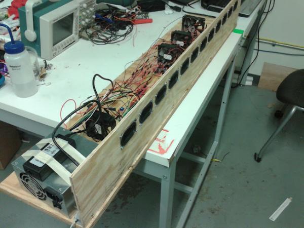
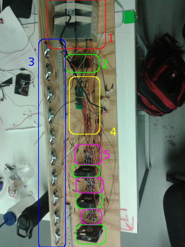
The entire setup was constructed from two scrap pieces of plywood held together with two aluminum box-beams. Holes were cut in one of the pieces the size of the speakers using a Dremel tool, and the speakers were constrained using four 4-40 screws and nuts each. The exact dimensions of the plywood are not important, as long is there is sufficient room for the full array of speakers and all the electrical components. The power supply was attached to the board with zip-ties, and the fan supply was taped on top of that. The boards were all held in place by stand-offs drilled through the board. The fans were restrained by hot glue. In the photo below, (1) is the power supply, (2) is the fans, (3) is the speakers, (4) is the input amplifier, ADC, microcontroller, and DAC, (5) is the speaker amplifiers, there are 4 per board.
Input Amplifier
The initial amplifier is designed to re-bias and amplify the audio input of -1 to 1V to 0 to 5V and is drawn below.
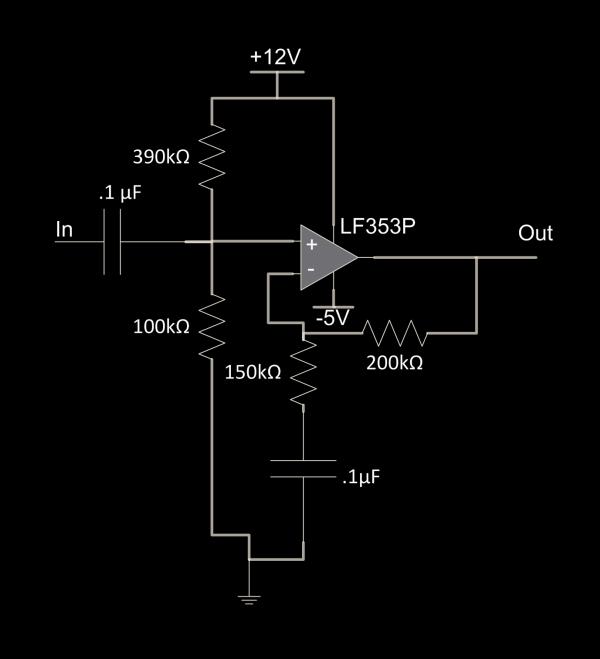
The first stage is a high-pass filter and re-biasing circuit, implemented by the first capacitor and the resistor divider. The corner frequency of this input high-pass filter is 1RC=1.1μF 80kΩ=125Hz1RC=1.1μF 80kΩ=125Hz. This is lower than the frequency response of our speakers, which is 200Hz, so it will allow all important frequencies through. The resistor divider between 12V and ground lowers the voltage to 12V100kΩ100kΩ+390kΩ=2.44V12V100kΩ100kΩ+390kΩ=2.44V. Since we want the zero-amplitude wave to be centered at 2.5V, this does a good job.
The second stage of the input amplifier is implemented with an LF353P Op-Amp in a non-inverting topology, and it amplifies only the high-frequency components due to the capacitor between the lower resistor and ground. The amplification factor is 1+R1R2=1+200kΩ150kΩ=2.331+R1R2=1+200kΩ150kΩ=2.33 for high frequencies. This will turn our -1 to 1V swing into a -2.33 to 2.33 V swing, which gets us near the rails, specifically to .11V and 4.77V. The corner frequency for this high-pass gain is 1RC=1.1μF 250kΩ=40Hz1RC=1.1μF 250kΩ=40Hz, which is high enough to block DC amplification, but low enough to amplify the frequency range we are interested in.
An interesting problem while building this stage was that initially the op-amp would rail too easily. This only allowed us to get a voltage swing of about 1.5 to 3.5V, which was lower than we wanted. Instead of solving this by finding a different op-amp, we realized we had voltage rails available to us higher than 5V and lower than 0V. Using those prevented the op-amp from railing, but if one were building a system where only 5V is available, a different op-amp with less overhead should be substituted. Furthermore, it is important to note that the op-amp have a fast enough slew-rate to track a 22kHz sine wave from 0 to 5V.
Analog Digital Converter (ADC)
The purpose of the ADC is to sample the input audio signal and transmit it to the microcontroller. Its schematic is found below.
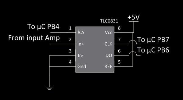
The ADC we used was the TLC0831. We used this ADC because it sampled just fast enough for us, was easy to use, and we were able to sample it for free. It is connected to the microcontroller via the standard SPI lines. We want the serial clock to be low when idle, which corresponds to CPOL = 0, and we want to sample on the leading edge and setup on the falling edge, which is equivalent to CPHA = 1. Since there is no possible configuration for this ADC, it only has a data out line. Therefore, it doesn’t matter what is written to SPDR, as writing any value will activate the serial clock and read values in from MISO. There is one important note about this ADC, and it can be seen from the SPI timing diagram from the datasheet.
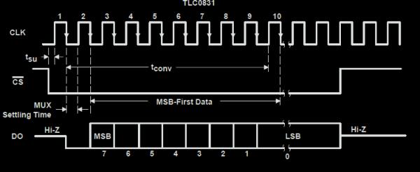
Notice the number of clock cycles in in the data transmission. It takes 10 cycles to transmit the 8 bits of data. Unfortunately, it is not possible to have the ATmega 644 run the SPI clock a custom number of times, it must be a multiple of 8. Therefore, two bytes must be written to SPDR to get the full ADC value back, and the bits must be shifted and stored appropriately.
If another ADC is substituted, the important parameters are that it be 8-bit, have a range from 0-5V, and can sample and communicate the result at a rate of at least 44.1kHz, preferably a little faster to allow for additional flexibility.
Microcontroller Setup
The microcontroller used in this setup is the ATmega 644. Another microcontroller could be substituted. The requirements are that the microcontroller must have at least 13 I/O pins, 1 ADC input, and SPI capabilities. Also, it must be able to run the SPI faster than 44.1kHz. The code is written using the AVR macros so different chips can be substituted by compiling with different chips selected in AVR studio. The microcontroller should be connected to power, decoupling capacitors, and an external crystal as recommended by Atmel. The crystal used in this setup should be 20MHz. Below is a table of the port connections of the microcontroller.
| Microcontroller pin | Connection |
|---|---|
| Pin A7..5 | A0..2 of both DAC chips |
| Pin A4 | !WR of DAC 2 |
| Pin A3 | !WR of DAC 2 |
| Pin A3 | Wiper of potentiometer between +5V and Gnd |
| Pin B7 | CLK of ADC |
| Pin B6 | DO of ADC |
| Pin B4 | !CS of ADC |
| Pin C7..0 | D7..0 of both DAC chips |
Digital to Analog Converter (DAC)
The DACs we used were two Maxim MX7228 octal, 8-bit DACs. The schematic for how we hooked them up is below.
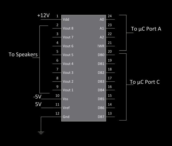
The MX7228 is a parallel DAC. What this means is the output voltage is a function of the 8-bits set to DB0..7. Given an 8-bit value x, the MX7228 sets the output to (Vref−Gnd)∗x256(Vref−Gnd)∗x256. The output that is set is defined by the 3 address bits, A0..2, and the register is written when the !WR line is pulled low. The existence of the !WR line allows us to address both DACs from the same 3 pins of the microcontroller and still maintain independent control of all 12 speakers. The code order for writing to one output channel is (1) Set Port C to desired output value, (2) Set Port A to the correct address and pull one !WR low, (3) Set Port A to pull both !WR lines high.
One important issue we ran across with this DAC is that when we were originally applying 5V to Vdd and 0V to Vss the output was unable to achieve the entire 5V range. Fortunately, we had a 12V and -5V rail available to us, and by applying these we were able to achieve the full desired range of the DAC.
If a substitution is desired, the DAC must be fast enough that 12 channels can be written at a rate of 44.1kHz, or preferably faster to allow more flexibility. This usually means a parallel-input DAC should be used, since even at a high SPI frequency it takes more time to write to a serial DAC than a parallel one, and there is not a shortage of output ports on the Microcontroller.
Speaker Amplifier
To drive the speakers, we needed an additional stage after the DAC. Our speaker amplifier is below.
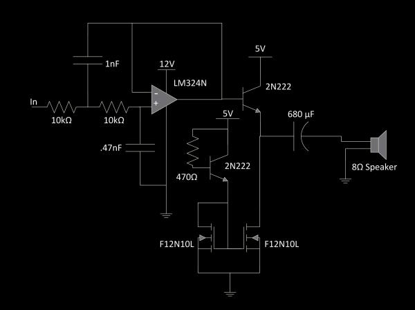
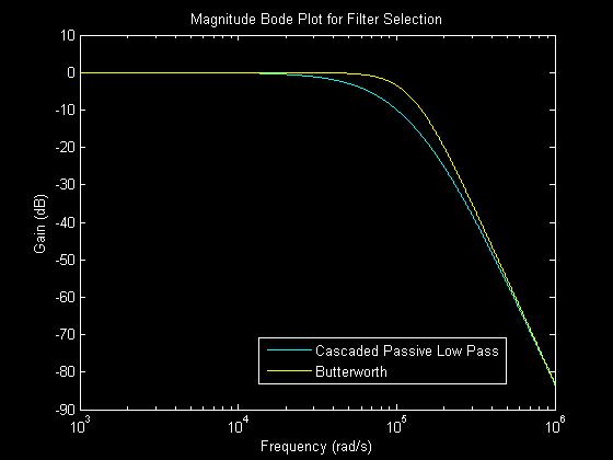
Although a DAC can produce a sine wave by producing the analog values there is a still quantization noise produced since the output of a DAC is not continuous over the output range. Therefore a second order Butterworth low pass filter is implemented to reject all frequencies that are not in the audible region. The filter is implemented using the Sallen-Key topology and the resistors and capacitors are selected so the cutoff frequency is about 23kHz.
A Butterworth filter was selected over cascading two passive RC filters because cascading two RC filters has a gain of -6dB at the cutoff frequency and the output of the signal would need to be buffered before being fed into the common collector amplifier. By using a Butterworth filter the filter is closer to an ideal low pass filter and the signal is buffered as Sallen-Key topology was used. Sallen-Key topology has a very large input resistance and a very low output resistance which is ideal for buffering a signal.
When selecting the op-amp for the filter the main parameter that has to be taken into consideration is the slew rate. An op-amp with a really high slew rate may be necessary if the application is dealing with frequencies above the human range of hearing. For audible frequency ranges a slew rate of 0.5VμsVμs was sufficient. One way to determine if the slew rate of the op-amp is not fast enough for the circuit is if a buffer is designed using the op amp. If a sinusoid wave is passed through the input of the buffer and the output is a triangle wave then the slew rate is too low for the circuit application. The LM324N is a quad op amp package that is sample-able from TI which was used for implementing the low pass filter. Each IC would filter four channels from the DAC that would be sent to the speakers.
The output of the filter is then passed to a common collector amplifier. A common collector amplifier has the following current gain, voltage gain, and output resistance:
The speaker is connected in series to a 680μFμF capacitor to create a high pass filter that was aimed at getting rid of the DC-bias of output signal. The equation for a high pass filter implemented with a passive RC circuit is as follows:
where R is the resistance of the speaker which is 8ΩΩ. This creates a cutoff frequency of about 30Hz. The capacitor that was used for the high pass filter was an aluminum polarized capacitor. It is fine to use a polarized capacitor as long as the voltage drop across the capacitor is smaller than what the voltage rating of the capacitor. The capacitor used was rated to 10V which is fine since the sinusoid being fed into the speaker has an amplitude of about 4V.
The reason a common collector amplifier is needed to drive a speaker is because the speaker has a very low impedance. Therefore any circuit that drives the speaker will need a low output impedance otherwise there will be a significant voltage drop since the circuit forms a voltage divider. To improve the linearity and efficiency of the amplifier a current source should used in place of the emitter resistance.
To implement a current source a NPN transistor is biased to act as a reference current by connecting a 430 ΩΩ between the base of the transistor and the 5V rail. The current outputted by the emitter of the NPN transistor is then fed into a current mirror implemented by two N-channel MOSFETs. The current mirror essentially copies the reference current and outputs the reference current through the other MOSFET which is connected to the common collector amplifier.
MOSFETs were selected over BJTs for the current mirror because there is no current flowing through the gate of a MOSFET, but there is a current flowing through the gate of a BJT. This causes a BJT to have the following equation for the current mirror:
The MOSFET current mirror equation is simply Icopy=IREFIcopy=IREF. These equations are based off of the assumption that the two transistors used in the current mirror are identical to each other. However transistors tend to have a large variation in their parameters caused by manufacturing. Transistors tend to have less variation in their parameters if array packages are used. Ideally a package with two transistors in the package would have been used. However, due to budget constraints it was cheaper to get individual MOSFET packages.
When selecting the MOSFET for the current mirror it is important to use a MOSFET that has a low RDSRDS. A high RDSRDS will limit how much current will be flowing through the reference current side of the current mirror. An RDSRDS smaller than 1 ΩΩ is small enough to allow sufficient current to flow through the NPN BJT being used as a current reference and improve the performance of the common collector amplifier.
Since the emulated current source replaces the emitter resistor, the emitter resistance becomes infinite which means that the voltage gain and output resistance equations change to the following:
Since the source of the input signal for the common collector amplifier is the output of a Sallen-Key topology the RsourceRsource value is almost zero. Also the value of β0β0 is in the range of 100 to 1000 so the term Rsourceβ0Rsourceβ0 is effectively zero. The term gmgm can be calculated with the following relation:
where ICIC is the DC collector current and VTVT is the thermal voltage which is typically around 26mV. With the speakers being driven at around 0.75A we see that gmgm is about 3 Ω−1Ω−1 which means that the output resistance of the amplifier is much smaller than the impedance of the speaker which allows most of the voltage drop of the signal be across the speaker and not somewhere else on the amplifier circuit.
This resistor was selected by using a potentiometer to see where the output signal of the common collector amplifier looked identical to the filtered input signal. Lowering the current limiting base resistor would improve the quality of the output signal, but would increase total power consumption and cause the NPN and N-channel MOSFETS to become significantly hot.
Unfortunately, with the transistors selected, the output signal did not produce an accurate representation of the original input signal unless the current limiting base resistor was relatively low causing the transistors to get hot. This is very problematic since this allows thermal runaway to occur. Thermal runaway in BJT transistors are caused by the fact that the leakage current of a BJT increases as the temperature increases. A positive feedback loop is formed since as the leakage current increases, the total current flowing through the transistor increases. As the total current increases the temperature increases, which then increases the temperature. Thermal runaway in MOSFETs occurs since as the temperature increases the on-resistance of the MOSFET increases. This causes more power to be dissipated on the on MOSFET since P=I2RP=I2R which increases the temperature.
Thermal runaway could be observed by looking at the current drawn by the amplifier circuit. As the circuit would be left running the current drawn by the circuit would steadily increase and the transistors would get hotter. A cooling system was implemented by adding a series of 12V power supply cooling fans in a way that create constant airflow across all the amplifier circuits. To keep isolation between the fans and the microcontroller a separate power supply from the computer power supply was used.
At first an isolating DC/DC was used to create the isolation. The PTB78560C (sample-able from TI) would take 24V from the power supply (implemented by using the 12V and -12V rails) and output an isolated 12V, by using the correct feedback resistors and capacitors that were mentioned in the datasheet. However, the output power of the DC/DC was not strong enough to power all the fans. Instead of using multiple DC/DCs to split up the number of fans powered by each DC/DC a PA-215 switching adapter was used to supply us an isolated 12V rated to 21.6W of power.
Results
Software Execution
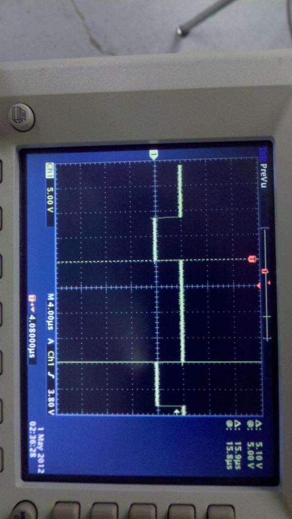
Due to our clever use of time in our ISR, our code runs smoothly with no delays or problems. There is no discernable delay in the input potentiometer – changing it changes the delay to the speakers immediately. Furthermore, it was measured that our ISR was executing at 44.15kHz using an oscilloscope and toggling a debug pin upon entering and exiting the ISR. By looking at the following waveforms we can see what the microcontroller enters and exits in the expected amount of time. Since all of the main processing power is done in the ISR for computing the time delays and values to output to the DAC we can measure the CPU usage percentage by looking at the duty cycle of the waveform. The high side of the duty cycle is 15.9μμs and the total time was measured to be 22.7μμs giving us a CPU usage percentage of 70.04%.
Accuracy
Overall, designing a phased array speaker system was successful as we were able to correctly implement group delay on all twelve speakers within the amount of time during the interrupt handler to manage sampling the music. The following waveforms show the group delay between speakers in the phased array and the amount of time the microcontroller spends in the ISR for updating the speakers based off of the sampled music.
Source: Phased Array Speaker System
- What does the system sample the audio at?
The system samples audio at approximately 44.1 kHz (implemented as 44.15 kHz). - How many speakers are in the array?
The array consists of 12 independently controllable speakers. - Can beam steering be achieved for wide-band audio with pure time delay?
Yes; MATLAB simulation and derivation showed wide-band beams can be steered using pure time delay without frequency-dependent phase adjustments. - What microcontroller was used and what are its key requirements?
An ATmega644 was used; requirements include at least 13 I/O pins, one ADC input, SPI capability, and the ability to run SPI faster than 44.1 kHz. - Why were parallel-input DACs chosen instead of SPI DACs?
Serial SPI DACs were too slow given MCU SPI limits and ADC timing; parallel DACs allowed updating all channels quickly (~1.2 μs) to meet interrupt timing. - How is the audio input rebias and amplified for the ADC?
An input amplifier rebiases the ±1 V audio to 0–5 V using a resistor divider and a high-pass stage, then an LF353P non-inverting amplifier provides gain for high frequencies. - What filtering is applied after the DACs?
Each channel uses a second-order Butterworth Sallen-Key low-pass filter with cutoff about 23 kHz to remove DAC quantization noise. - How was thermal runaway handled in the amplifier stage?
Cooling fans scavenged from computers were used to provide airflow to keep amplifier transistors from overheating. - What user interface is provided to change beam steering?
A potentiometer read by the microcontroller ADC selects one of nine delay bins controlling delay between speakers. - What timing technique avoided heavy bounds checking in ISR buffer indexing?
Modulo addressing via power-of-two buffer length (2048 bytes) with bitwise AND masking (0x07FF) was used to allow roll-over without bounds checks.