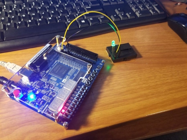
This tutorial will show you how to turn on an LED using both the built-in LED on a development board as well as using a GPIO pin. I happen to be using a DE0 CV Dev board from Terasic. We will be using the Quartus design environment to do this.
Software Requirements
– Quartus design environment found here
– USB blaster drivers (they should be included in the Quartus download)
Hardware Requirements
– FPGA Dev Kit
– LED with resistor (330ohm- 1kohm should be fine)
Step 1: Project Setup (1)
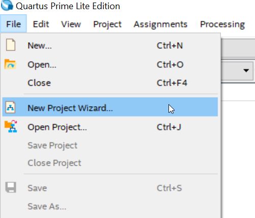
Create a new project in Quartus
Step 2: Project Setup (2)
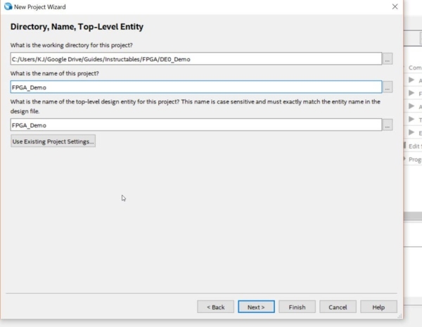
Set your save locations
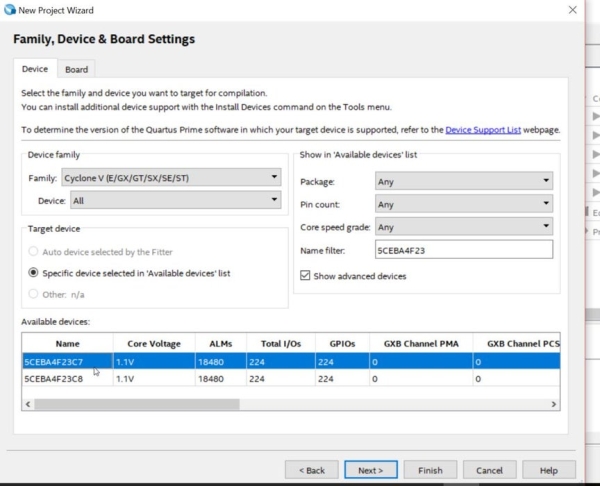
Step 3: Project Setup (3)
– Select empty project type
– Click next on the add files screen
– Select your chip
Step 4: Project Setup (4)
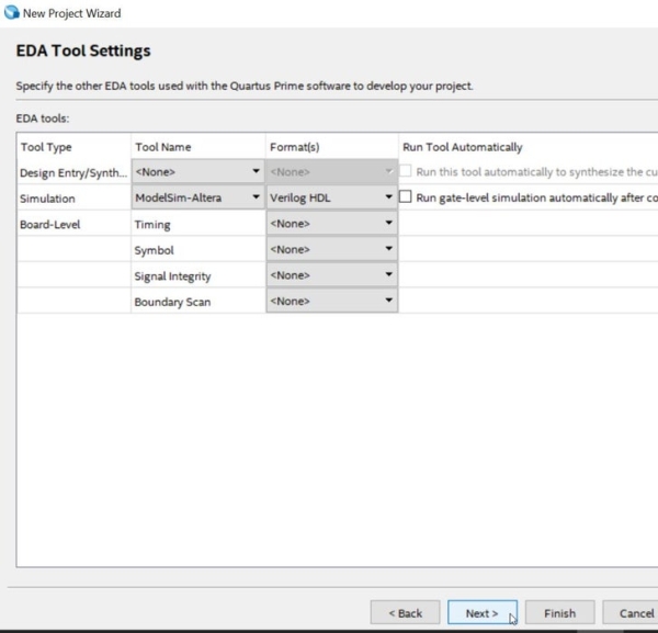
-Select your tools
– Click finish
Step 5: Project Setup (5)
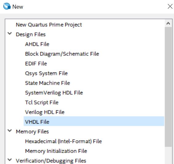
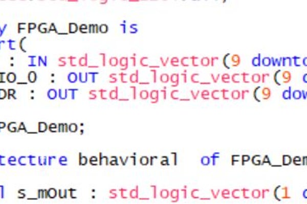
– Create new vhdl file
– Copy the code below into it
–START
library ieee;
use ieee.std_logic_1164.all;
entity FPGA_Demo is
Port(
SW : IN std_logic_vector(9 downto 0);
GPIO_0 : OUT std_logic_vector(9 downto 0);
LEDR : OUT std_logic_vector(9 downto 0)
);
end FPGA_Demo;
architecture behavioral of FPGA_Demo is
signal s_mOut : std_logic_vector(1 downto 0);
begin
process(SW)
begin
s_mOut <= SW(9 downto 8);
end process;
GPIO_0(0) <= s_mOut(1);
LEDR(8) <= s_mOut(0);
end behavioral;
–END
Step 6: Add Your Board’s .qsf
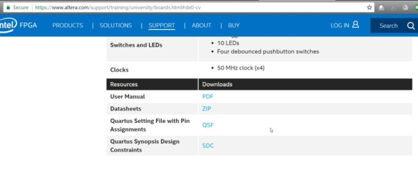
– The QSF file sets the pin assignments for your board.
– using this link you may be able to find the .qsf file for your dev kit…download it.
Step 7: Import Pin Assignments
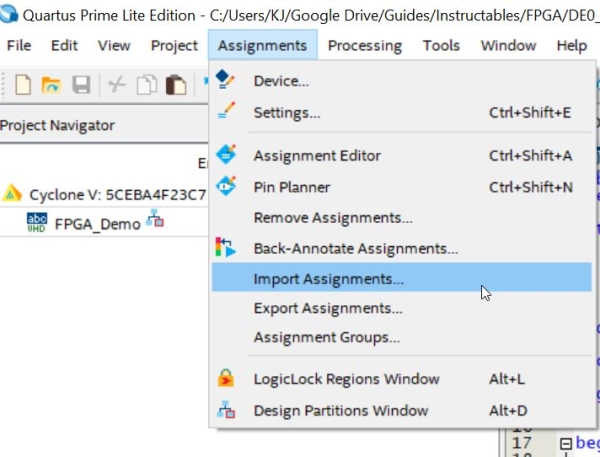
Import the pi n assignments and select the .qsf file you just downloaded
Step 8: Configure Your Pins
I happen to have a board with 10 LED and switches as well as 2 2×20 GPIO headers. Your board may be different. You may need to check some of the PORT settings in the .vhdl file and make sure they will work with your board.
I have configured the GPIO_0(0) and GND pins to my resistor on the breadboard. The code is sett up assuming this and may need editing to make it work for you.
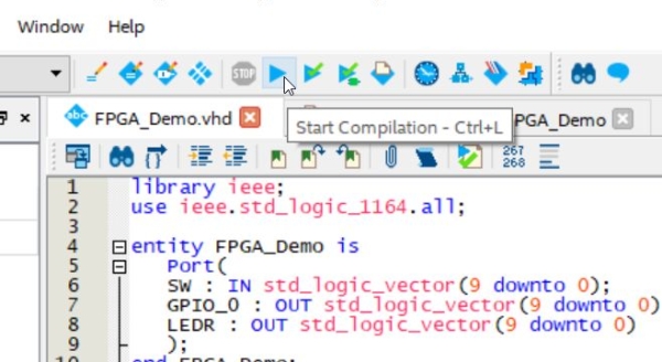
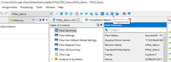
Step 9: Compile Project
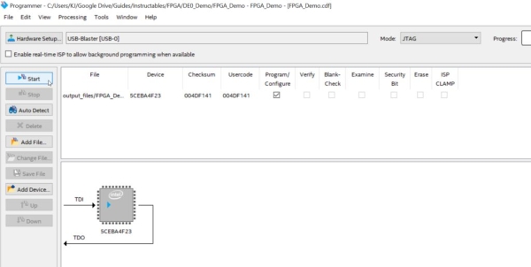
Step 10: Open the Programmer
Step 11: Download Program to Chip
Step 12: Wrap-Up
Hopefully you should have a working circuit by now. FPGAs can be quite tricky so your setup may have created obstacles along the way. just post a comment and we’ll see if we can help out.
Hope this helps!
Source: Simple Altera FPGA Demo