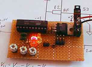
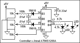
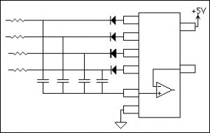
The test circuit (schematic below, photograph above), when running the associated firmware (click here to see the assembler code (file name “hfcm030602.asm”), compares two test voltages, appearing on the wires of the 10k pots, with a reference voltage, which appears on the wiper of the 50k pot. When a test voltage exceeds the reference voltage, the LED corresponding to that particular test voltage lights, demonstrating that the two sampled channels are independent.
The AT90S1200A used for the test has a single comparitor, but an analog multiplexer was formed using two of its digital bidirectional I/O ports. Notice that for each analog input, there is a 100k resistor, a .01 uf capacitor, and a diode. The resistor-capacitor combination form a low pass filter and switching of the charged capacitor is the means by which multiplexing is effected.
Here is how it works
The technique takes advantage of bidirectional I/O ports to switch from outputs to inputs. In the case of many AVR controllers, the input of the comparitor shares a pin with a bidirectional I/O bit. This allows the pin to be held at ground and then ungrounded when using it as an input for the comparitor.

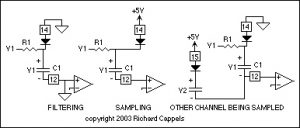
When it is time for the input voltage to be connected to the comparitor input, pin 12 is opened (the I/O pin is made into an input) and the multiplexing pin, pin 14, is connected to + 5V (made into an output pin and written with a logic high). This causes the positively charged plate of the capacitor to be connected to +5V through the diode. This results in a a Vdd minus one diode drop, minus the voltage on the capacitor being applied to pin 12.
Vpin12 = the voltage applied to the analog input of the comparitor, pin 12,
Vdd = the power supply voltage, 5 volts in this example,
Vdiode = the voltage drop across the diode, which is somewhat dependent on the current through the input resistor, and
Vin = the input voltage applied to the input of the RC filter.
One thing that should be apparent from looking at the expression above, is that input voltages are restricted to the range of 0 volts to Vdd-Vdiode, or 0 to about 4.4 volts. As voltages approach 4.4 volts, the current through the diode will become very low, and a noticeable linearity may develop.
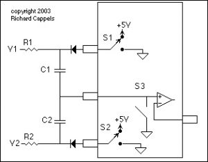
To make a multiplexer, simply combine two or more of these switched capacitor stages along with their control I/O pins, as shown in the illustration below.
The diodes are necessary to provide isolation while the other channels are selected. In the third state illustrated below, the voltage V2 across a second channel is being sampled. If the V2 = 0 volts, and if V1 = 5V (so that the voltage across C1 = 5 volts), then when V2 is sampled, the cathode of the connected to pin 15 is one diode drop below the +5V supply, and that would put the positive plate of the C1 at about +9.4 volts. The diode in series with the multiplexing pins (14 and 15 in this example) is there to isolate the high positive voltages from the internal protection circuitry in the microcontroller.
As many channels as needed may be added by simply adding an additional resistor, capacitor, diode, and output pin for each channel.
Firmware to switch and sample the comparitor’s input
The routine below is called by a timer interrupt every 2048 clock cycles.

	cbi	DDRB,0		;+ Input to comparitor high Z.

	sbi	PORTB,2		; Input 1 pin logic high.
	nop			; Wait 1 microsecond for comparitor to settle.
	in	LED1,ACSR	; Copy comparitor state to memory.
	cbi	PORTB,2		; Input 1 pin logic low.

	sbi	PORTB,3		; Input 2 pin logic high.
	nop			; Wait 1 micrsecond for comparitor to settle.
	in	LED2,ACSR	; Copy comparitor state to memory.
	cbi	PORTB,3		; Inputnel 2 to logic low

	sbi	DDRB,0		; + Input of comparitor to ground.
In the above code fragment, LED1 and LED2 refer to internal RAM registers associated with inputs 1 and 2 respectively. Care must be taken to make the I/O port bit associated with the comparitor input into an input before switching the signals to the diodes, else the voltage across the capacitors be disturbed. Then entire source code for the AT90S1200A is included in the file hfcm030602.asm.
Mischarge if filter capacitor and resulting error
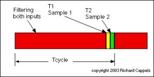
During the filtering period (see figures 4 and 6) the input resistor and associated capacitor are connected as a low pass filter. During the time input 1 is being sampled, the voltage across C1 does not change. During the sampling of input 2, the voltage on C1 is disturbed by a “mischarge” through R1. The formulae to analyze this depend upon the type of input filter used. A fast filter, in which the RC time constant of the filters is small compared to the total measurement cycle time (Tcycle in Fig. 7) will allow more responsiveness in detecting voltage changes. Filters with long RC time constants compared to Tcycle can give better accuracy at the expense of responsiveness. The point at which one gives better accuracy than the other depends on the actual Tcycle, T1, and T2 times. Ways to analyze both are described.
If the time constant of R1C1 is large compared to the total measurement cycle time, the amount of mischarge (cross talk) is proportional to the ratio of the input voltage times its duty cycle to the other channels voltages times their duty cycles. The maximum cross talk voltage, Vmc1max =(Vdd – Vdiode) (T2/(Tcycle)
Where
Vct = volts across C1 (output of multiplexer) resulting from mischarge during sampling of other channels,
Vdd = power supply voltage,
Vdiode = voltage drop across multiplexing isolation diode,
T2 = time in which input 2 is sampled, and
Tcycle = the period of one total measurement cycle.
This shows how measurement frequency can be traded against mischarge. Keep the measurement periods (T1, T2, etc.) as short as possible and keep the measurement cycle (Tcycle) as long as necessary to maintain the required isolation between channels.
The mischarge error across C1 for a given case can be found by: Vmc1 =( (V2-Vdd-VC2) T2)/(Tcycle-(T1+T2))
Where
Vmc1 = mischarge voltage error across C1,
V2 = voltage into input 2 of the multiplexer (V2 in figure 5),
Vdd = power supply voltage,
T2 = time in which input 2 is sampled,
Tcycle = the period of one total measurement cycle, and
T1 = time in which input 12 is sampled.
It is practical to use the expression for Vmc1max for design purposes and the expression Vmc1 for the purpose of analysis.
In the example code, interval between measurements are 2048 clock cycles, as set by the timer interrupts, and the time spent measuring each channel is 3 clock cycles. Accordingly, with Vdd = 5.0 volts, and assuming Vdiode = 0.5 volts, the maximum offset is 6.6 millivolt, or 0.15% of the 4.5 volt full span signal.
If the RC time constant of the input filter short compared to the total cycle time, then the mischarge error can be calculated using the exponential resistor-capacitor charging formula. In the case of a two input multiplexer, the worst case occurs on the second channel to be sampled, which in the case of this example is input 2. At the end of the charging period, C2 is charged to Vin2. During T1, the voltage across C2 changes as C1 is switched to Vdd.. The worst case is when Vin1 = 0 volts, so that there are 0 volts across C2, and the voltage on the negative end of C1 change by VDD-Vdiode. C1 And C2 are in series, so if their capacitances are equal, the effective capacitance = C2/2 and the voltage change across C2 is half the total voltage change across the series capacitance. The maximum error,
Verror = (Vdd-Vdiode) (1 – (exp ( -T1 / ( R2 ( C2 / 2) ) ) ) ) / 2
In the case of this example, where the input filters are made of 100k resistors and .01 uf capacitors, Vdd = 5.0 VDC, Vdiode = 0.5 volts, and T1 = 3 microseconds (1 MHz clock for the microcontroller), the maximum error is 13.5 millivolts, or 0.3% of the 4.5 volt full span signal.
One other effect to take note of, is that the switching signal will appear on the inputs of the multiplexer. This will range from zero to (Vdd-Vdiode) peak-to-peak through the input resistor. This may have an effect on the circuit being monitored.
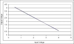
The result of a test
The data below was measured on the test circuit:
Procedure:
1. Set Vin.
2. Adjust Vref just until the LED associated with Vi illuminated.
3. Record Vref voltage.
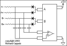
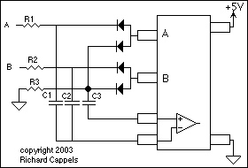
If an additional I/O port is available to reset the capacitor, one of the diodes can be eliminated.
For more detail: Analog Multiplexer using AVR microcontroller

