What’s inside a TTL chip? To find out, I opened up a 74181 ALU chip, took high-resolution die photos, and reverse-engineered the chip.1 Inside I found several types of gates, implemented with interesting circuitry and unusual transistors. The 74181 was a popular chip in the 1970s used to perform calculations in the arithmetic-logic unit (ALU) of minicomputers. It is a moderately complex chip containing about 67 gates and 170 transistors3, implemented using fast and popular TTL (transistor-transistor logic) circuitry.
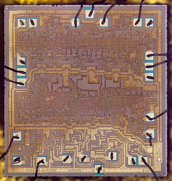
The 74181 die photo is below. (Click the image for a high-resolution version.) The golden stripes are the metal layer that interconnects the circuitry of the chip. (It’s not gold, just aluminum that looks golden from the lighting.) The white squares around the edge of the die are the pads that are connected by tiny bond wires to the external pins. Under the metal layer is the silicon that makes up the chip. Faint lines show the doped silicon regions that make up the transistors and resistors. While the chip may appear impossibly complex at first, with careful examination it is possible to understand how it works.
The 74181 chip is important because of its key role in minicomputer history. Before the microprocessor era, minicomputers built their processors from boards of individual chips. The arithmetic operations (addition, subtraction) and logical operations (AND, OR, XOR) were performed by the arithmetic/logic unit (ALU) in the processor. Early minicomputers built ALUs out of a large number of simple gates. But in March 1970, Texas Instruments introduced the 74181 Arithmetic / Logic Unit (ALU) chip, which put a full 4-bit ALU on one fast TTL chip.4 This chip provided 32 arithmetic5 and logic functions2, as well as fast carry lookahead.7 Using the 74181 chip simplified the design of a minicomputer processor and made it more compact, so it was used in many minicomputers. Computers using the 74181 ranged from the popular PDP-11 and NOVA minicomputers to the powerful VAX-11/780 to the Datapoint 2200 desktop computer. The 74181 is still used today in retro hacker projects.6
A brief guide to NPN transistors
The 74181 is built from bipolar NPN transistors, a different technology from the MOS transistors in modern processors. The diagram below shows how an NPN transistor appears in an integrated circuit, along with a cross section. The transistor has three connections: the collector, base and emitter, with metal lines for each. The collector is connected to N-type silicon, the base to P silicon, and the emitter to N silicon (giving it the NPN structure). On the chip, you can recognize the emitter from its nested squares, the base because its silicon region surrounds the emitter, and the collector because it is the largest contact.
The key idea of the NPN transistor is it acts as a switch between the collector and emitter, controlled by the base. Normally there is no current flow between the collector and the emitter, so it’s like a switch in the “off” position. But if you pass a small current from base to emitter, the transistor allows a large current from collector to emitter, like a switch in the “on” position. (This is vastly oversimplified—bipolar transistors are much more “analog”—but should be enough to understand how the 74181 works.) At the right is the symbol for an NPN transistor with the collector, base and emitter labeled.
Inverter
The fundamental component of TTL logic is the inverter, and other gates are modifications of the inverter circuit. Thus, it’s important to understand the basic construction of the inverter, even though it is a bit complicated. I’ll explain how it works in an oversimplified way.9
The diagram below shows an inverter in the 74181 chip. The 5V and ground lines run vertically along the left, powering the inverter. The transistors are highlighted with boxes. The resistors are visible as long strips of doped silicon snaking around.11 An input pin (A0) is wired to the pad. On the right is the schematic for a TTL inverter10, with components highlighted to match the die photo.
Read more: Inside the 74181 ALU chip: die photos and reverse engineering