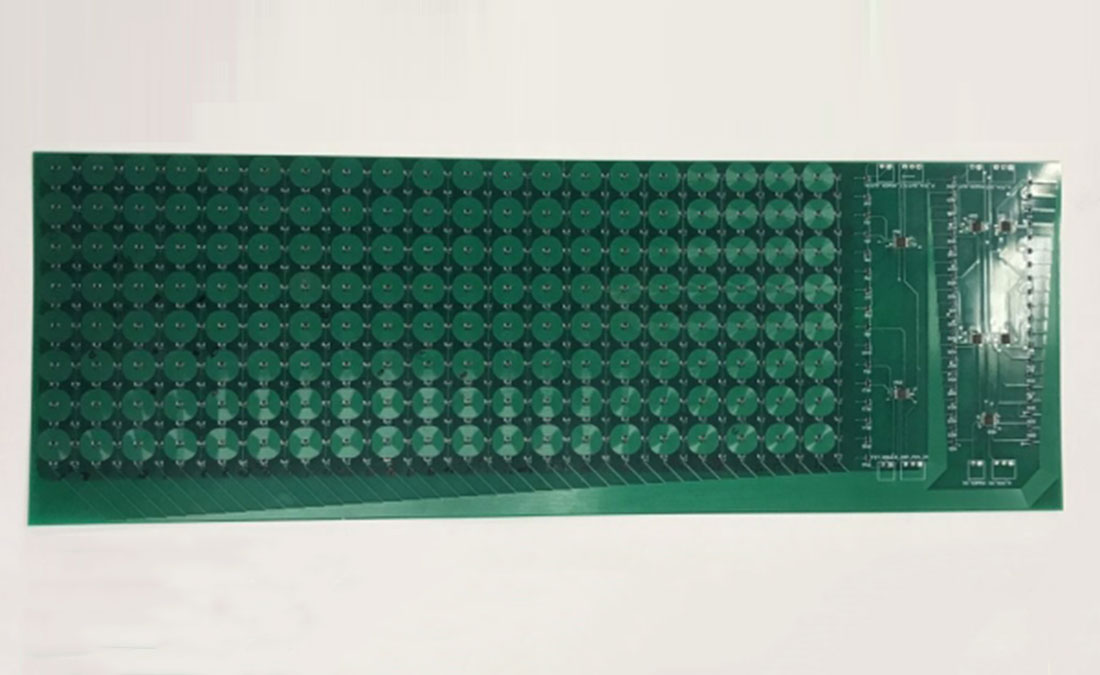
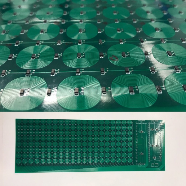
This past summer I had the opportunity to work for computer science PhD candidate Ryo Suzuki under the guidance of Tom Yeh of the computer science department. My task was developing printed circuit boards for experiments for human computer interaction (HCI). The goal was to create a surface which a magnet could be moved to create patterns, animations, display information and alerts. Below is an image of the coil array, dispersed on 4 layers. This allows for tighter resolution. By having over lapping coils, the magnet could be pulsed and moved in less discrete steps. The further the coils are apart, the more discrete each position appears, resulting in less smooth transitions, and increased current to attract the magnet from point A to point B.
After all of the setbacks and stress, this was a tremendous experience. I have finally learned Altium Designer and I have learned how to use it well. A project of this scale was imperative to learning Altium’s features thoroughly and introduced me to more manufacturing considerations for future projects. I am happy to have had the opportunity to work under pressure and guidance of such a driven individual. Below, I talk about my discoveries and adventure with Altium Designer 17.
The PCB is an array of coils alternating layers so that the distance between centers of coils could be minimized. This would allow for the smoothest possible actuation of the magnetic marker. A current is pulsed through individual coils allowing for the magnet to be pushed smoothly across the top of the board. The array is similar to an LED matrix, where a P and N type FET pair are used to activate a specific coil. Shift registers were used to allow for more coils to be used with a single micro controller (Arduino). The control of the system was designed by Ryo with some input from myself. Essentially we we tried to maximize the surface area we could cover, the goal was a desk space, as we thought that this would provide an interesting medium for humans to interact.
This was a challenging project that allowed me to grow professionally and improve my PCB fabrication skillset. My main task for this project was to create a 4 layer circuit board, iterating on the previous design developed by Ryo. This project was challenging for a few reasons. One, I was learning Altium Designer 17, and two, I did not comprehend the scalability when designing in Altium. The list of major hurdles overcome in this project included:
- Custom part footprints- coils with 10 mm diameter, 8 mil spacing.
- Via placement while minimizing coil placement
- Scaling 16 coils to 2560 coils
- Optimizing designs to allow Altium to handle the large number of primitives in each coil
This project highlighted the importance of addressing small problems found in the schematic. It may appear that a problem could be fixed with 3 clicks, but when scaling to larger designs, 3 clicks may quickly grow to thousands of time consuming and incident prone clicks. It is important to spend time upfront to ensure the schematic is correct before attempting layout.
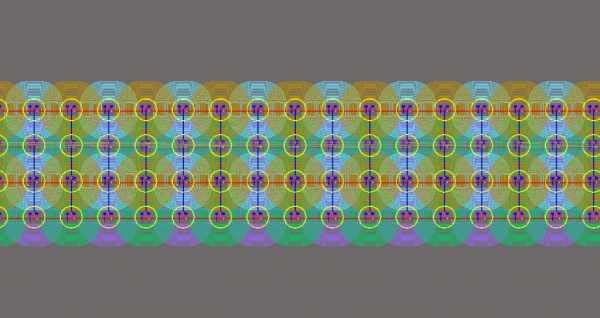
The first iteration of the board used only 8 coils on 3 layers, which failed to work with the control system, but it did provide insight on design. Altium and our computers were able to handle this board without issue. I noticed that the coils created using Planar-TX (script) resulted in many primitives (lines and arcs) that appeared to be connected but failed to be electronically, resulting in many short circuit warnings. I initially ignored this because I knew that the circuits were electronically connected and only the spacing mattered. Turns out the hundreds of primitives resulted in Altium becoming very slow and unresponsive. The solution was to use Planar-Tx to create the coil, but then create a custom component so that the primitives became one, thus becoming one electronically connected component.
The board was easily manipulated in layout to fix all the “small” issues such as mislabeled nets, additionally generated nets, and short circuits. This board had only 9 coils.
When scaling this up for 3200 coils, it was apparent that the fixes from the pervious round would not be viable. A redesign was required. After consulting the internet and Professor Alex Fosdick, the solution was found by creating custom foot prints consisting of rows and using rooms. Learning about rooms was the coolest feature I have ever used. It allows for a routing and placement of components to be repeated easily, regardless of the complexity of the layout. An upfront cost is required to properly set up the schematic with schematic sheet symbols, but after this the savings is immense
Prior to the board being created, we checked the sizes produced by our manufacturer and requested a quote. We were under the understanding the quote we used was validated by a human and would allow for the maximum size of our board to be made. Unfortunately it was found that the quote was not accurate and was only so for 4 layer boards of rigid material less than 500 mm in length. Our hopes for using flexible pcb was crushed. Another redesign was required. Some time was spent on the possibilities to reduce costs, maintain control surface area, and feasibility of a redesign. Already the board was behind schedule and magnitudes more challenging than originally anticipated. Through many emails with the manufacturer, we decided we could still get the surface area of the board if the boards were split among four PCBs with 80 x 16 coils each.
Source: Summer 2017 Altium Designer 17 Research