Summary of 3 channel, 8 bit EEPROM DAC with DS interface using ATtiny12 microcontroller
The article describes a low-power, low-cost device using an ATtiny12 microcontroller that offers three channels of 8-bit pulse-width modulation (PWM) DAC outputs with 16 bytes of onboard EEPROM for autonomous operation. DAC values can be programmed via a DS interface and stored in EEPROM for automatic reloading at power-up, making it ideal for setups without microcontrollers. It includes hardware considerations for output filtering to minimize ripple and guidance on pin connections to avoid interface issues. The device is positioned as a cost-effective alternative to EEPROM DACs and potentiometers.
Parts used in the 3 channel, 8 bit EEPROM DAC with DS interface using ATtiny12 microcontroller:
- ATtiny12 microcontroller
- Resistors (including 100k resistor for reset)
- Capacitors (for RC output filters)
- Power supply (typically 5V or lower)
- DS interface pins
- Low power.
- EEPROM memory for autonomous operation, 16 bytes available for general purpose use.
- Low cost.
This device provides three channels of 8 bit pulse-width modulation. Output pulse duty cycle ranges from 0 to 255/256 in 255 steps. DACs may be loaded by the DS interface. DAC values may also be copied into the on-chip EERPOM and then automatically be loaded into the DACs when power is applies, making it useful for automatic set up of circuits that do not contain microcontrollers. This replaces more expensive EEPROM DACs and EEPROM pots in many applications, owing to its use of a small area high volume integrated circuit microcontroller. Additionally, one page of 16 bytes of on-chip EEPROM storage is accessible via the DS interface.
Pinouts of the DAC. Avoid long parallel traces or flat ribbon cable runs with the PWM0 and Attention line signals in parallel in such a way that the PWM0 signal couples heavily into the Attention line as this signal could make the interface hang up .
Downloads
Code
AVRStudio assembler source (HTML -copy and paste to assembler editor)
AVRStudio hex file
MACAVRpa hex file
When programming the chip it is recommended elect internal oscillator and set the brownout detector to the high voltage consistent with your application.
Short form user guide dsdacmap.pdf (36k file)
Hardware considerations
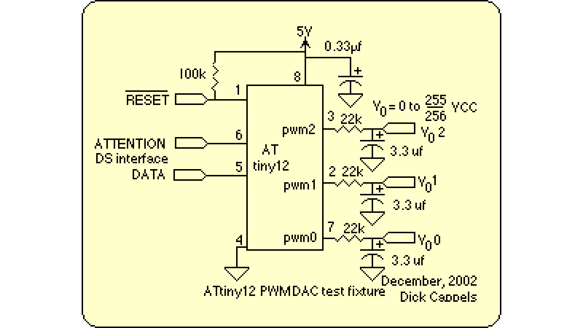
With the values for the RC (resistor-capacitor) filters given on the schematic above, the worst case ripple will be about 1/2 lsb at 5V. Lower power supply voltages casue the ATtiny12’s osciallator frequency to dorp. Thus to maintain 1/2 lsb ripple. It would be necessary to increase the resistors or the capcaitors in the output filter.
If during reset initialization, the EEPROM checksum is found to be correct, the DAC values stored in EEPROM will be loaded into the DACs. As such, the DS interface pins can be permanently tied to ground if the situation calls for it. Similarly, if the reset input is not used, the 100k resistor may be omitted and pin 1 tied directly to VCC. If the reset input is tied directly to VCC check the final assembly language code carefully to make sure that DDRB bit 5 is never set as an output and PB5 is never driven low because port B bit 5 is an alternative function of pin 1.
This DS slave device does not have any internal pull-ups. This chip uses the same PWM generation method as the 8 channel 8 bit DAC. See this page for details of operation.
It should be noted that the VCC of the PWM DAC needs to be close to the VCC of the host. Check the device’s respective data sheets for details.
For more detail: 3 channel, 8 bit EEPROM DAC with DS interface using ATtiny12 microcontroller