Introduction:
We thought it would be interesting to try and construct a simple modem out of the ATMEL 8535. The main motivation for doing this was to test some DSP theories about the effects of transmission power, noise, and modulation technique on the bit error rate. Initially, we wanted to connect our modem to the public telephone network; however, the voltage, current, and bandwidth constraints over a phone line would have made the project much more complex. Instead, we chose to use a simple wire channel, and focus our efforts on actually transmitting and receiving the signal waveform.

High Level Design:
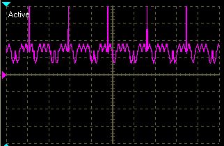
Our goal was to make our modem so that it would be full duplex and we would be able to send and receive characters over a noisy analog channel. For simplicity, we chose to use the UART and Hyperterminal on a PC to provide data to the modem, and display the output of the receiver. The characters were to be transmitted pseudo asynchronously by transmitting a high voltage synchronization pulse, one parity bit, then the eight data bits. This allowed for a high level of fault tolerance because the transmitter and receiver are synchronized at the beginning of every byte. Binary �1�s were to be transmitted by a waveform with values defined in a table so that we could easily change the waveform. To transmit binary �0,� we simply negated the values in the table. We varied the number of samples per bit transmitted as well. To receive the signal the MCU waits for expected high voltage of the sync pulse. It then waits for the end of the sync pulse to begin sampling the bits. The reciever uses a correlator algorithm to detect whether the received signal was a binary ‘0’ or ‘1.’ We varied the number of samples per bit to evaluate the tradeoffs between speed and noise tolerance.
Transmitter
When a byte is received from the UART, the transmitter starts the transmit sequence begins by with a sync pulse. This is a short spike of five volts that signals to the receiver that a byte is coming. Following the sync pulse, the transmitter calculates a parity bit to ensure that the number of �1�s transmitted is even. The parity bit is transmitted as a waveform over the channel, followed by the eight data bits. To control the speed of the transmitted, we used the timer one compare match interrupt. Every interrupts, a new sample of the waveform corresponding to the bit is loaded from flash and sent to the DAC. Since we were using BPSK, we only needed to store one waveform in flash, since we could just negate the value to produce the waveform for a binary zero. Also, since we didn�t want to deal with negative voltages, we introduced a digital DC offset into out transmission. The DC offset was added to the value to be transmitted at the transmitter and subtracted at the receiver. This allowed us to avoid the added complexity of more external hardware, while still being able to use BPSK.
For more detail: Analog Modem Design Project