The project which we are presenting is not the project we presented in our proposal. We initially planned to build a WWVB time-code receiver, which would demodulate a 60 kHz signal and extract an extremely precise time according to the National Institute of Standards and Technology (NIST). Unfortunately, due to a weak signal and noise interference, we decided that a time-code receiver would not be feasible to build. Instead we chose to design our project around a laptop hard drive that Richard had in his possesion. After studying the capabilities of the hard drive, we decided to build a hard drive based microcontroller programmer.
The basic function of the microcontroller programmer is to allow a user to select between several ROM files stored on the hard drive and then program the selected ROM file into a target MCU. Design of the programmer would incorporate features of microcontroller-based design such as serial communication and the use of LCDs as seen in lecture, as well as new concepts such as reading from a FAT32 partitioned hard drive.
High Level Design
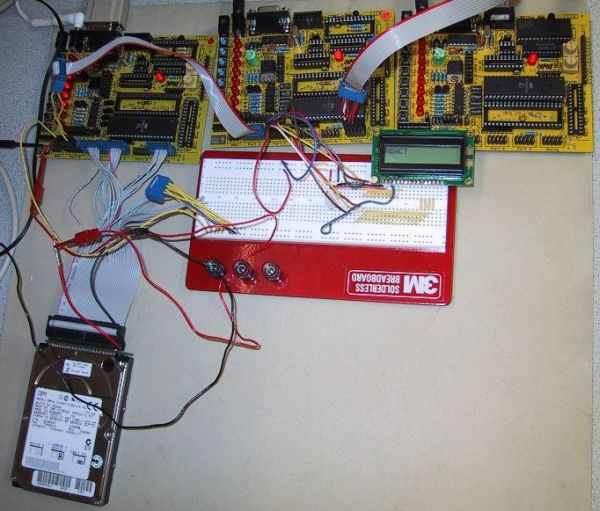
The goal of our project was to created an MCU programmer that read ROM data from a standard IDE hard drive. Our design conisted of two ATMEGA163 microcontrollers communicating in a master-slave relationship. The slave MCU controlled a FAT32 laptop hard drive, while the master MCU handled user input (push buttons) and output (an LCD display) as well as progamming the target MCU. We chose to restrict our target MCU to an AT90S8515 because it only requires a single instruction to program its flash while the mega163 requires two instructions. The figure below shows the relationship between all the major components of our system.
We would have liked to ideally used only one microcontroller but the interface to the hard drive required 24 i/o pins alone. The LCD requires an entire port (8 pins), 4 i/o pins are needed to program the target MCU, and a minimum of two pins are required to get user input. All of these i/o requirements exceeded the 36 pins provided on a single 8515 or mega163.
To establish communication between the two MCU’s, we wired their UARTs together. On power up the slave MCU does a hard reset of the hard drive and performs a listing of the root directory. The most critical information about each file (name, file size, and first cluster) is stored in an array in memory. The slave then goes into an infinite loop and waits for a request from the master MCU.
When the master MCU powers up, it sends a request to the slave for a list of all the file names it found. The master then displays the first file on the LCD and enters a a state machine to debounce button presses from the user. The user can cycle through the files and each is respectively displayed on the LCD. When the user presses the program button, the master sends the index of the file currently selected to the slave. The slave MCU responds to this request via its UART receive complete interrupt. It then reads the file from disk and streams the contents to the master.
The format of the ROM file is that produced by the CodeVison compiler. An example of that format is shown below.
00000D:0000
00000E:94F8
00000F:27EE
000010:BBEC
000011:BFE5
000012:E1F8
000013:BDF1
000014:E1F0
000015:BDF1
Each line gives a memory address (the first six characters) followed by the value to be programmed at that address (the last four characters). Since ROM files can be quite large they would easily exceed the SRAM in a mega163, as a result we only buffer one line at a time and program each word in memory as it is streamed into the master. The master converts the ascii hex values to integers and progams the target MCU in-system by sending commands and data serially to the targets RESET, MOSI, MISO, and SCK pins.
Hardware Design
The slave MCU is connected to 24 lines of the hard drive. The drive can be completely controlled from only these connections despite the 40 pins provided on the device. Of these 24, the majority correspond to the 16-bit bi-directional data bus (HD00-HD15) of the drive. By reconfiguring the direction of the port pins we were able to perform both reads and writes without the need for multiplexing or tri-state buffers. The remaining 8 pins corresponded to the 3 address select lines (HA00-HA02), the 2 chip select signals (HCS0-HCS1), reset (HRESET), read (HIOR), and write (HIOW). The signal CSEL was connected to ground to permanently configure the drive as device 0 or master. In addition the hard drive has 7 other pins that are grounded (pins 2, 19, 22, 24, 26, 30, and 40). The rest are left unconnected.
An important electrical consideration we encountered was the hard drive current spikes immediately after power up. As a result we had to use an AC/DC power adapter (5V) that could source at least 1 amp otherwise the drive would never initialize.
To establish communcation between the slave and master, the TXD pin of each MCU was connected to the RXD pin of the opposite device.
The LCD was connected to the master MCU and controlled using the LCD libraries provided by CodeVision. A potentiometer was installed across Vcc and ground to adjust the contrast of the display.
Finally, the GND, RESET, MISO, MOSI, and SCK pins supplied at the ISP header on the STK200 board used to program our target MCU, were connected to output pins of the master.
For more detail: Hard Drive Based AVR Programmer