For my Word Clock project, for which I built a custom 8 x 8 LED Matrix with controller, I needed a much smaller footprint DIY-Duino (board for an ATMega328P microprocessor), one that would have all of the main functionality of my previous DIY-Duino boards (such as the Arduino Uno I2C Master board). As I’m not going to include I2C in the Word Clock, I can get rid of that without compromising the board and secondly, I can add an ICSP sub-board without it taking up any space in the clock.
So, that’s it, the design brief. A smaller custom Arduino that can be served by an add-on ICSP sub-board to make programming the microprocessor easy.
The parts:
Barebones Arduino
• 1 x ATMega328P
• 2 x 10 uF Electrolytic Capacitors
• 2 x 0.01 uF Ceramic Capacitors
• 1 x LM7805 Voltage Regulator
• 1 x 16 MHz Crystal
• 1 x Tactile Momentary SPST switch
• 1 x 1K ohm resistor
• 1 x 28 pin DIL socket
• 2 x 6 pin female headers
• 2 x 8 pin female headers
• 1 x 30 mm x 62 mm PCB (Single Sided)
ICSP Sub-Board
• 4 x 3 pin male headers
• 1 x 6 pin male headers
• 1 x 27 mm x 48 mm PCB (Single Sided)
I had made the board with connection for my USB Serial Adapter, but that doesn’t seem to work … here are the parts if you are interested.
• 1 x 6 pin male headers
• 1 x 0.01 uF ceramic capacitor
Well, it turns out that the reason that the USB Serial Adapter connection didn’t work is that my Freetronics USB Serial Adapter is fried. So, it wasn’t my ICSP Sub-board that wasn’t working.
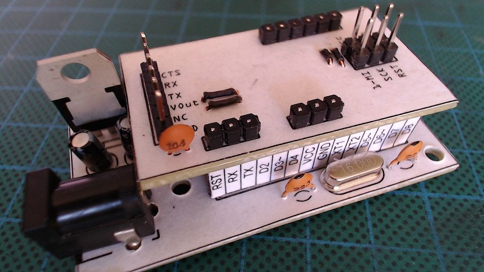
Step 1: Barebones Arduino No FTDI
Normally, I don’t bother with the reset button … I decided to keep the button “in” for this project.
As there is very little space on the board for labels, I made up two small labels in MS-Word for the pins and glued them directly onto the female pin headers.
As usual, solder the lower parts first, resistors, crystal, ceramic capacitors and then the taller parts, electrolytic capacitors, DIL socket, female headers, power socket and then the LM7805.
Once these are in place, the two jumpers are connected between the switch and reset (pin 1) and between pins 8 and 22 (GND).
At this point, you should get out your multimeter and test trace continuity across the board and then, with the power connected (but without the ATMega328P chip installed) test the functionality of the voltage regulator. When you’ve tested the board and it is all OK … put the ATMega328P chip into the socket.
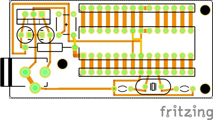
 Fritzing – ATMega328P Board – No FTDI – Small Footprint_etch_copper_bottom.pdf
 - Fritzing – ATMega328P Board – No FTDI – Small Footprint_etch_silk_top.pdf

Step 2: ICSP Sub-board
This is a very simple sub-board that is used to upload sketches onto your ATMega328P and is removable so that it doesn’t take up valuable real-estate in your enclosure.
The sub-board simply connects the ICSP pins to the ATMega328P.
| Function | Pin | Pin | Function |
| MISO | 18 | 7 | VCC |
| SCK | 19 | 17 | MOSI |
| RESET | 1 | 8/22 | GND |
For more detail: Small Footprint ATMega328P Board