Pinout Diagram for Atmega32 AVR
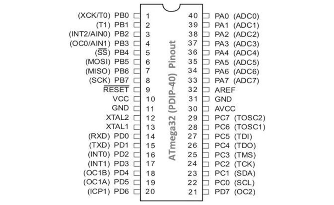
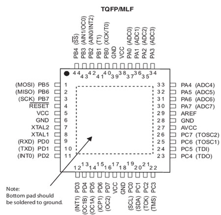
Complete guide and explanation for atmega avr pinout. Atmega32 is built on CMOS (Complementary metal–oxide–semiconductor) technology which has high speed, low power consumption and enhanced anti-static effects. Pin counts are different for different packages but with almost same characteristics.
- PB-0: T0 (Timer/Counter External Counter Input ) can also be used as XCK (USART (also known as serial port) External Clock Input/Output)
- PB-1: T1 (Timer/Counter1 External Counter Input) can also be used as INT2 (External Interrupt 2 Input)
- PB-2: AIN0 (Analog Comparator +(Positive) Input) can also be used as INT2(Interrupt) (External Interrupt 2 Input)
- PB-3: AIN1 (Analog Comparator -(Negative) Input) can also be used as OC0 (Timer/Counter0 Output Compare Match Output)
- PB-4: SS (SPI Slave Select Input Pin)
- PB-5: MOSI (SPI Bus Master Output/Slave Input Pin)
- PB-6: MISO (SPI Bus Master Input/Slave Output Pin)
- PB-7: SCK (SPI Bus Serial Clock Pin)
- RESET: Master Device Reset this pin is active low
- VCC: Power Supply Pin Voltage input range is 2.7V – 5.5V for ATmega32L and 4.5V – 5.5V for ATmega32
- GND: Power Supply Ground Reference 0v
- XTAL2: External Crystal Pin 2
- XTAL1: External Crystal Pin 1
- PD-0: RXD (UART Input Pin)
- PD-1: TXD (UART Output Pin)
- PD-2: INT0 (External Interrupt 0 Input Pin)
- PD-3: INT1 (External Interrupt 1 Input Pin)
- PD-4: OC1B (Timer/Counter1 Output CompareB Match Output Pin)
- PD-5: OC1A (Timer/Counter1 Output CompareA Match Output Pin)
- PD-6: ICP (Timer/Counter1 Input Capture Pin)
- PD-7: OC2 (Timer/Counter2 Output Compare Match Output Pin)
- PC-0: SCL ( 2-wire Serial Bus Clock Line Pin)
- PC-1: SDA ( 2-wire Serial Bus Data Input/Output Line Pin)
- PC-2: TCK ( JTAG Test Clock Pin)
- PC-3: TMS ( JTAG Test Mode Select Pin)
- PC-4: TDO ( JTAG Test Data Out Pin)
- PC-5: TDI ( JTAG Test Data In Pin)
- PC-6: TOSC1 ( Timer Oscillator Pin 1 )
- PC-7: TOSC2 ( Timer Oscillator Pin 2 )
- AVCC: This is power supply source for port A, It must be connected with Vcc if not using ADC, It has also another feature for ADC i.e. noise reduction through low pass filter supply from vcc.
- GND: Power Supply Ground Reference 0v
- AREF: Reference Voltage pin for Analogue to digital converter(ADC)
- PA-7: General Purpose Digital Input/Output and can also be used as ADC(Analog to Digital Convertor) input channel 7
- PA-6: General Purpose Digital Input/Output and can also be used as ADC(Analog to Digital Convertor) input channel 6
- PA-5: General Purpose Digital Input/Output and can also be used as ADC(Analog to Digital Convertor) input channel 5
- PA-4: General Purpose Digital Input/Output and can also be used as ADC(Analog to Digital Convertor) input channel 4
- PA-3: General Purpose Digital Input/Output and can also be used as ADC(Analog to Digital Convertor) input channel 3
- PA-2: General Purpose Digital Input/Output and can also be used as ADC(Analog to Digital Convertor) input channel 2
- PA-1: General Purpose Digital Input/Output and can also be used as ADC(Analog to Digital Convertor) input channel 1
- PA-0:General Purpose Digital Input/Output and can also be used as ADC(Analog to Digital Convertor) input channel


