Summary of Building a Web Server Using AVR Microcontrollers
This article describes implementing an embedded web server using an 8-bit AVR microcontroller (ATmega32) and an ENC28J60 Ethernet controller, covering hardware, SPI interfacing, networking protocols (TCP/IP, IP, TCP, HTTP), cabling, and miscellaneous components and power regulation. It explains system architecture, interfacing, and protocol stack concepts needed to host simple web pages and remotely control devices.
Parts used in the AVR Web Server:
- Atmel ATmega32 Microcontroller
- ENC28J60 Ethernet Controller
- Integrated Magnetics RJ-45 Jack (MagJack) with AutoMDIX
- RJ-45 connector / Ethernet cabling (10BASE-T twisted pair)
- LM7805 voltage regulator (5V)
- LM317 adjustable voltage regulator (3.3V)
- JHD-162A 16x2 LCD display (HD44780U driver)
- Passive components for ENC28J60 interface (pulse transformers or integrated magnetics, resistors, capacitors)
- SPI connections (MISO, MOSI, SCK, SS) between ATmega32 and ENC28J60
On this occasion, I express my gratitude to the Almighty for bestowing His grace upon me, leading my efforts to a successful conclusion. I extend heartfelt thanks to my esteemed mentor, Mr. Vinod Kumar P.P., whose invaluable guidance and advice steered me through crucial moments, illuminating the right path. I sincerely appreciate the support extended by Dr. David Peter, the esteemed head of the division, for granting me access to the available facilities.
I would also like to acknowledge and thank the other faculty members for their contributions. Lastly, but certainly not least, I express my profound appreciation to my friends and family for their unwavering support and encouragement throughout the duration of my work.
INTRODUCTION
This section offers an introductory overview of embedded web servers and their implementation. It elucidates their typical application through illustrative examples. Section 1.2 succinctly outlines the implementation process of an embedded web server based on the Atmel AVR microcontroller.
1.1 Embedded Web Server
From small-scale setups to larger systems, interfaces and controls are commonly accessible either through onboard switches or via IR or RF-based remote control. However, a scenario arises when a user, desiring control over a device, is physically distant or located in another part of the world. Although various remote control methods have been developed, each necessitates unique implementations. In this context, we leverage the established technique of the Internet Web using the HTTP protocol within the TCP/IP protocol suite to enable remote device control. This incorporation of a web application within a system is termed as an embedded web server.
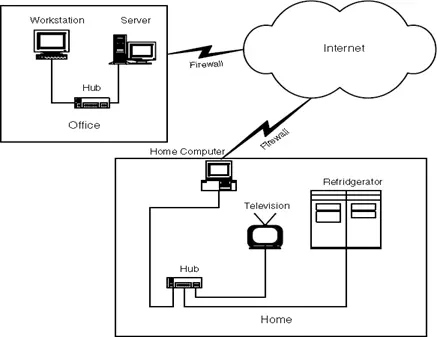
Consider an arrangement where an Embedded Web Server is integrated into multiple units within a household, as depicted in Figure 1.1. Each server maintains a connection to the network. A home-based computer, illustrated in the figure, serves as a central control hub for all devices and remains open to requests from other computers over the Internet. Each web server is identified through its distinct IP address, allowing remote control from any location globally.
For instance, a computer situated in an office might transmit a request via the Internet to turn off the Refrigerator located at the user’s home. The web server, operating an HTTP application, enables users to control and monitor devices through its interface, thereby facilitating remote management.
1.2 8-bit Microcontroller based Web Server
Employing a web-based interface to regulate or supervise a device isn’t a novel concept. Numerous commonplace devices already leverage this methodology in daily life. Examples include printers connected through Ethernet links and remote surveillance cameras, among others. However, most of these devices utilize 32-bit processors such as ARM, AVR32, COLDFIRE, POWER ARCHITECTURE, among others.
The utilization of these 32-bit microprocessors inevitably escalates the expenses associated with an application. Remarkably, for the implementation of a basic Embedded Web Server, it’s entirely plausible to utilize 8-bit Microcontrollers, presenting a more cost-effective alternative.
The subsequent diagram at a higher level elucidates the process of implementing a web server on an 8-bit Microcontroller.
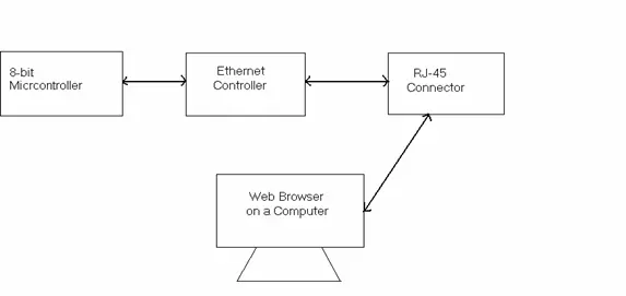
Figure 1.2 illustrates the connection between an 8-bit microcontroller and an Ethernet controller responsible for managing the physical layer of the TCP/IP stack model. Using a standard RJ-45 connector, the Ethernet controller interfaces with a PC. When a request is initiated from a web browser, it undergoes transmission as raw bits through the Ethernet lines and is subsequently received by the Ethernet controller. The Ethernet controller then forwards this information to the microcontroller. The program executing on the microcontroller decodes the request and executes the necessary operations.
Utilizing an 8-bit AVR Microcontroller streamlines the design process. Among the widely used 8-bit AVR Microcontrollers is the ATmega32, featuring 32 Kb of Flash memory, sufficiently capacious to store a small web page.
In the forthcoming sections, we’ll delve into a system study, addressing diverse hardware and software requisites pertinent to the project.
SYSTEM STUDY
This section involves conducting a comprehensive system study encompassing the examination and analysis of diverse hardware, software prerequisites, and limitations. Within Section 2.1, attention is directed towards outlining the hardware prerequisites while elucidating the associated constraints, which can be resolved through the selection of alternative hardware components.
Moving to Section 2.2, the focus shifts to the exploration of networking essentials essential for formulating various protocols. This encompasses a study of protocols such as TCP, IP, HTTP, ICMP, among others.
Transitioning to Section 2.3, a concise introduction is provided regarding the software packages employed in the process.
2.1 Hardware Study
To establish a web server on an 8-bit Microcontroller, we’ve opted for the AVR microcontroller due to its commendable throughput capabilities. In this setup, we’re utilizing the ENC28J60 Ethernet controller instead of the Realtek Ethernet controller family. The ENC28J60’s limited pin count makes it more conducive for easy interfacing with the 8-bit Microcontroller.
We’ll provide a concise overview of several pivotal components as follows (Further study can be pursued through their respective datasheets):
– Atmel ATmega32 Microcontroller.
– ENC28J60 Ethernet Controller.
– Integrated Magnetics RJ-45 Jack.
Additionally, we’ll delve into the miscellaneous components utilized in this setup. Furthermore, we’ll explore the usage of SPI (Serial Peripheral Interfacing) employed for interfacing the ATmega32 with the ENC28J60.
2.1.1 Atmel ATmega32 Microcontroller
A microcontroller is a compact chip housing all the essential components of a controller within its structure. Generally, these components encompass a CPU, RAM, a type of ROM, I/O ports, and timers. In our specific application, we’ve chosen to employ the ATmega32 as an 8-bit microcontroller. This selection is primarily due to its commendable throughput and its capability for SPI (Serial Peripheral Interface) interfacing. The SPI interface offers a serial link with the device, effectively reducing the number of address and data lines required.
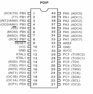
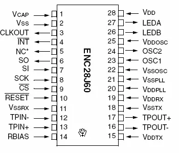
2.1.1.1 PIN Configuration
2.1.1.2 Overview
The ATmega16 microcontroller operates as a low-power CMOS 8-bit system, utilizing the AVR enhanced RISC architecture. Its capability to execute robust instructions within a single clock cycle enables the ATmega16 to achieve throughputs nearing 1 MIPS per MHz. This feature grants system designers the flexibility to balance power consumption against processing speed. Figure 2.2 depicts the block diagram illustrating its architecture.
The AVR core boasts an extensive instruction set along with 32 general-purpose working registers. Each of these 32 registers maintains a direct connection to the Arithmetic Logic Unit (ALU), enabling the simultaneous access of two independent registers within a single instruction, executed within a single clock cycle. This architectural design enhances code efficiency, leading to throughputs that can achieve speeds up to ten times faster compared to conventional CISC microcontrollers.
The ATmega32 encompasses the key functionalities below:
– Capable of achieving up to 16 MIPS Throughput at 16 MHz
– Embeds an on-chip 2-cycle Multiplier
– Provides 32K Bytes of In-System Self-programmable Flash program memory
– Includes 1024 Bytes of EEPROM
– Contains 2K Bytes of Internal SRAM
– Supports In-System Programming via an On-chip Boot Program
– Features a JTAG (IEEE std. 1149.1 Compliant) Interface
– Offers Two 8-bit Timer/Counters with Separate Prescalers and Compare Modes
– Incorporates One 16-bit Timer/Counter featuring Separate Prescalers, Compare Mode, and Capture Mode
– Integrates a Real-Time Counter with a Separate Oscillator
– Provides Four PWM Channels
– Houses an 8-channel, 10-bit ADC
– Facilitates a Byte-oriented Two-wire Serial Interface
– Includes a Programmable Serial USART
– Offers Master/Slave SPI Serial Interface
– Provides a Programmable Watchdog Timer with a Separate On-chip Oscillator
– Incorporates an On-chip Analog Comparator
– Features an Internal Calibrated RC Oscillator
– Offers External and Internal Interrupt Sources
– Encompasses Six Sleep Modes: Idle, ADC Noise Reduction, Power-save, Power-down, Standby, and Extended Standby
2.1.1.3 AVR CPU Core
The primary role of the CPU core is to ensure accurate program execution. To accomplish this, the CPU needs to access memories, conduct computations, manage peripherals, and handle interrupts effectively. Figure 2.3 illustrates a standard AVR CPU core.
For optimal performance and parallelism, the AVR implements Harvard architecture, which employs separate memories and buses for program and data. Instructions stored in the program memory are executed using a single-level pipelining approach. As one instruction is underway, the subsequent instruction is pre-fetched from the program memory. This design allows for the execution of instructions in each clock cycle. Notably, the program memory utilizes In-System Reprogrammable Flash memory.
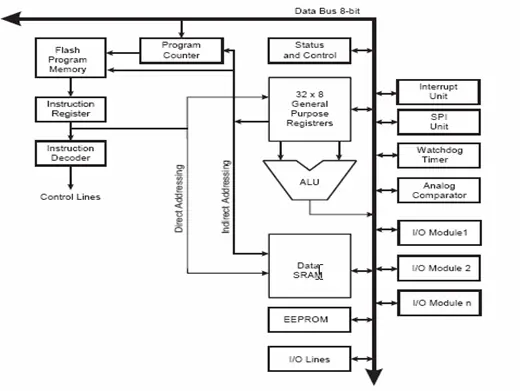
The Register File, designed for quick access, comprises 32 x 8-bit general-purpose working registers that can be accessed within a single clock cycle. Among these registers, six can serve as three 16-bit indirect address register pointers within the Data Space addressing system, facilitating streamlined address calculations.
The ALU (Arithmetic Logic Unit) enables arithmetic and logic operations either between registers or between a constant and a register. Additionally, single register operations can take place within the ALU. Post-execution of an arithmetic operation, the Status Register is promptly updated to reflect pertinent information concerning the operation’s outcome.
2.1.2 ENC28J60 Ethernet Controller
An Ethernet Controller serves to execute the Ethernet Protocol. The choice of the ENC28J60 as the Ethernet Controller in our application stems from its compatibility with SPI (Serial Peripheral Interface) interfacing. This SPI interfacing facilitates a serial interface with the device, consequently reducing the quantity of address and data lines utilized.
2.1.2.1 Pin Configuration
2.1.2.2 Overview
The ENC28J60 stands as an independent Ethernet controller equipped with an industry-standard Serial Peripheral Interface (SPI). It’s specifically crafted to function as an Ethernet network interface for any controller equipped with SPI. Compliant with all IEEE 802.3 specifications, the ENC28J60 integrates multiple packet filtering mechanisms to regulate incoming packets. Additionally, it houses an internal DMA module to ensure rapid data throughput and hardware-assisted checksum computation, crucial in various network protocols.
Communication with the host controller is established through an interrupt pin and the SPI, supporting clock rates of up to 20 MHz. Dedicated pins are allocated for LED indications, signaling link status and network activity. An illustrative block diagram of the ENC28J60 is depicted in figure 2.5. Remarkably, connecting a microcontroller to an Ethernet network using the ENC28J60 necessitates only two pulse transformers and a handful of passive components.
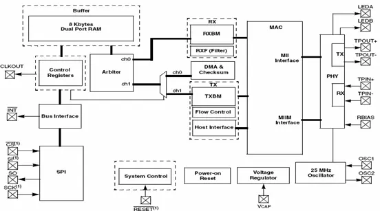
The ENC28J60 is comprised of seven primary functional blocks:
1. An SPI interface acts as the communication conduit linking the host controller to the ENC28J60.
2. Control Registers are employed for overseeing and managing the ENC28J60’s operations.
3. A dual port RAM buffer handles both incoming and outgoing data packets.
4. An arbiter regulates access to the RAM buffer when requests originate from DMA, transmit, and receive blocks.
5. The bus interface interprets and processes data and commands received via the SPI interface.
6. The MAC (Medium Access Control) module integrates IEEE 802.3 compliant MAC logic.
7. The PHY (Physical Layer) module encodes and decodes the analog data conveyed through the twisted pair interface.
Key features of the ENC28J60 include:
– Compatibility with IEEE 802.3 Ethernet standards
– Integration of MAC and 10BASE-T PHY
– Support for a single 10BASE-T port with automatic polarity detection and correction
– Compatibility with Full and Half-Duplex modes
– Programmable automatic retransmission in case of collisions
– Programmable padding and CRC generation
– Programmable automatic rejection of erroneous packets
– SPI Interface supporting clock speeds up to 20 MHz
A typical application circuit using the device is shown in the following figure 2.6
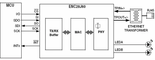
Only five lines suffice to establish the Microcontroller’s interface with the ENC28J60. Upon receiving a data packet, the ENC28J60 triggers an interrupt directed at the Microcontroller. The main program then inspects the received packet’s timing and determines its protocol. Subsequently, the program executes the necessary actions based on the identified protocol.
2.1.3 Integrated Magnetics RJ-45 Jack
2.1.3.1 Overview
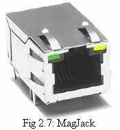
An RJ-45 Jack with integrated magnetics contains the necessary pulse magnetics within the jack unit. Ordinarily, a pulse transformer is combined with the RJ-45 jack to sustain the input pulse’s waveform and power while adjusting the source impedance to a value similar to the load impedance. Opting for an RJ-45 Jack with integrated magnetics eliminates the need for a pulse transformer in the circuit, thus avoiding the extra overhead involved in its use.
Figure 2.8 displays a common circuit configuration found within an Integrated Magnetics RJ-45. Meanwhile, Figure 2.7 showcases a standard Integrated Magnetics RJ-45 jack referred to as MagJack. Additionally, the MagJack offers a functionality known as AutoMDIX.
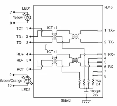
2.1.3.1 AutoMDIX
An Ethernet connection typically utilizes one wire pair for transmitting (Tx) and another for receiving (Rx). When employing a Hub/Switch, the signal is amplified and interconnected by linking the Tx of one network component with the Rx of the other. If the intention is to directly link the AVR web server to a computer without a Hub/Switch intermediary, a cross-connect Ethernet cable is usually necessary. This type of cable features a configuration where Tx and Rx are exchanged on one end.
The AutoMDIX magjack incorporates additional internal logic that automatically adjusts the cable as required, effectively swapping Tx and Rx if necessary. This means that regardless of whether we are connecting to a Hub/Switch or directly to a computer, we can consistently use a straight cable.
2.3.3 Cabling
The ENC28J60 is compatible with 10BASE-T transmission, indicating a data transfer rate of 10 Mbps. In this context, “BASE” refers to baseband, indicating that there’s no employment of frequency-division multiplexing (FDM) or other forms of frequency shifting modulation. Each signal retains complete control over the wire, operating on a single frequency. The “T” denotes the use of twisted pair cables, where wire pairs are twisted together to minimize crosstalk effects.
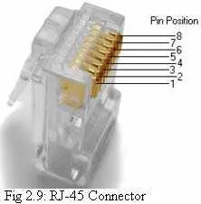
The transmission cabling employed utilizes 8-position modular connectors, commonly referred to as RJ-45 connectors in the realm of Ethernet over twisted pair (as depicted in figure 2.9). Typically, the cables utilized are four-pair or higher twisted pair cables. This standard accommodates both full-duplex and half-duplex communication modes. As per the standards, this system functions over distances of ‘up to 100 meters’.
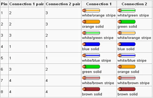
To establish a direct connection between two computers without utilizing a switch, an Ethernet crossover cable is commonly employed. Table 1 demonstrates the pin outs for a two-pair crossover cable, illustrating the connections at both ends of the cable. However, this limitation can be circumvented by employing the AutoMDIX feature of an RJ-45 Jack.
2.1.4 SPI (Serial Peripheral Interface)
2.1.4.1 Overview
The ATmega 32 Microcontroller employs the SPI (Serial Peripheral Interface) for efficient communication with the Ethernet controller ENC28J60. Utilizing SPI enables serial communication, reducing the number of lines typically needed for data and addressing purposes. This interface facilitates high-speed synchronous data transfer between the AVR and peripheral devices, as well as among multiple AVR devices. Additionally, in most instances, the SPI serves a dual function, being utilized for In-System Programming (ISP).
When connecting two SPI devices, one device operates as the master while the other acts as the slave. Unlike certain peripheral devices, such as sensors that solely function in slave mode, the AVR’s SPI can be configured to operate in both master and slave modes. The mode in which the AVR operates is determined by the settings of the master bit (MSTR) found in the SPI control register (SPCR). It’s essential to consider specific nuances regarding the SS pin during this configuration process.
The master functions as the active component within this system and is responsible for supplying the clock signal upon which serial data transmission relies. In contrast, the slave lacks the capability to generate the clock signal and cannot initiate actions independently. The slave’s role is limited to sending and receiving data only when the master provides the essential clock signal. Notably, the master generates the clock signal solely during data transmission. Consequently, for the slave to convey data, the master must initiate the data transmission process.
2.1.4.2 Data transmission between Master and Slave
The interaction between a master and a slave AVR is shown in the figure 2.10
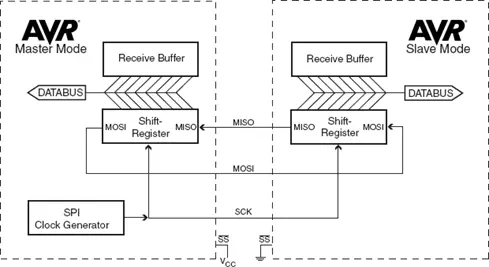
Two identical SPI units are depicted, with the left unit configured as the master and the right unit configured as the slave. The MISO, MOSI, and SCK lines are interconnected with their corresponding counterparts in the other unit. The operational mode of each unit determines whether these lines function as input or output signal lines.
Since a bit is concurrently shifted from the master to the slave and from the slave to the master within a single clock cycle, both 8-bit shift registers can be viewed as a unified 16-bit circular shift register. Consequently, after eight SCK clock pulses, data exchange between the master and slave occurs. The system is set up with single buffering in the transmit direction and double buffering in the receive direction.
This affects data handling in the following manners:
1. New bytes intended for transmission cannot be written to the data register (SPDR) or shift register until the entire shift cycle concludes.
2. Received bytes are promptly written to the Receive Buffer right after the transmission is finished.
3. To prevent data loss, it’s essential to read the Receive Buffer before the subsequent transmission completes.
4. Reading the SPDR will retrieve the data from the Receive Buffer.
Upon completion of a transfer, the SPI Interrupt Flag (SPIF) gets set in the SPI Status Register (SPSR). Enabling both this interrupt and global interrupts will trigger the execution of the corresponding interrupt. Activating the SPI Interrupt Enable (SPIE) bit in the SPCR enables the SPI interrupt, while setting the I bit in the SREG enables global interrupts.
2.1.4.3 Pins of the SPI
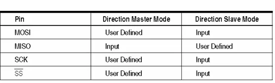
The Serial Peripheral Interface (SPI) comprises four distinct signal lines: the shift clock (SCK), the Master Out Slave In line (MOSI), the Master In Slave Out line (MISO), and the active low Slave Select line (SS). Upon enabling the SPI, the data direction of the MOSI, MISO, SCK, and SS pins is altered as outlined in the following Table 2.
2.1.5 Miscellaneous Components:
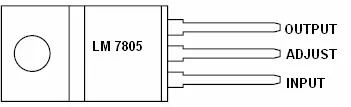
The LM7805 is a three-terminal positive voltage regulator that incorporates built-in features such as current limiting, thermal shutdown, and protection in its safe-operating area. These features render it highly resistant to damage caused by output overloads. In this context, we utilize the LM7805 to obtain the necessary 5V output required by the ATmega32 Microcontroller. Figure 2.11 illustrates the pin configuration of the LM7805 IC.
2.1.5.2 LM 317 IC
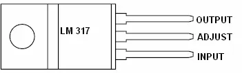
The LM317 represents an adaptable 3-terminal positive voltage regulator that can provide over 1.5A within an output range spanning from 1.2V to 37V. These regulators are notably user-friendly, necessitating only two external resistors to establish the output voltage. Additionally, both line and load regulation surpass that of standard fixed regulators. In this instance, we utilize the LM317 voltage regulator to achieve the 3.3V output needed by the ENC28J60 IC. The pin layout of the LM317 IC is depicted in Figure 2.12.
2.1.5.3 JHD-162A LCD Display
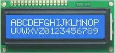
An LCD display provides extensive flexibility for users to showcase necessary data. It can serve as a debugging tool by indicating executed subroutines, displaying their values on the screen. In our scenario, a 16×2 alphanumeric LCD display is employed to exhibit the current AVR IP, the ADC value (if connected), and temperature data. The LCD driver acts as an intermediary between the microcontroller and the LCD. For instance, the JHD 162A LCD display utilizes the HD44780U driver. The inclusion of the header file in the program depends on the specific LCD display driver being utilized.
Figure 2.13 shows a JHD 162A LCD display
2.1.6 Interfacing of Different Components
The following figure shows the main interfacing of AVR web server:
2.2 Networking
Prior to composing a program for the ATmega32 microcontroller, it’s essential to acquaint ourselves with the TCP/IP protocol stack, Ethernet frame structure, and the Web browser protocol (HTTP). Each of these elements will be comprehensively discussed in this section, one by one.
2.2.1 TCP/IP Protocol Suite
The TCP/IP protocol suite enables computers of varying sizes and running diverse operating systems to establish communication among themselves. This protocol suite serves as the foundation for what is commonly referred to as the global Internet—a Wide Area Network (WAN) connecting millions of computers.
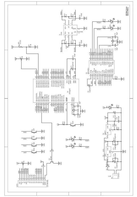
TCP/IP Suite Layers: The TCP/IP protocol suite is comprised of multiple protocols distributed across different layers. Typically acknowledged as a 4-layer system, TCP/IP encompasses various protocols across these layers, as illustrated in figure 2.15.
2.2.1.1 Application Layer
The Application layer manages the intricacies of a specific application, with typical TCP/IP applications encompassing:
• Remote login through Telnet
• Web page display via browser support
• File transfer applications
• Email applications
The three lower layers remain unaware of the specific application details, focusing solely on handling communication aspects.
2.2.1.2 Transport Layer
TCP ensures a dependable transmission of data between two hosts by breaking down the information received from the application into suitable segments for the underlying network layer. It acknowledges sent packets and retransmits lost ones, offering a reliable data flow. As the Transport Layer manages this reliability, the Application Layer can overlook these intricacies.
In contrast, UDP provides a more straightforward service to the Application Layer. It dispatches data packets, known as datagrams, from one host to another without assuring that they reach their destination. Any desired reliability needs to be implemented by the Application Layer itself.
2.2.1.3 Network Layer
This stratum is occasionally referred to as the Internet Layer, overseeing the transfer of packets within the network. Routing activities, such as packet navigation, occur within this layer. The Network Layer in the TCP/IP Protocol Suite is facilitated by IP (Internet Protocol) and ICMP (Internet Control Message Protocol).
2.2.1.4 Link Layer
The Data-link or Network Interface Layer is alternatively referred to by another common name. Typically, the Link Layer encompasses both the device driver within the operating system and the corresponding network interface (card) in the computer. Collectively, these components manage all the hardware intricacies involved in physically interfacing with the cable.
2.2.2 Combining all
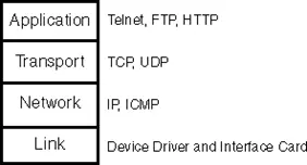
Figure 2.16 shows an example that includes two hosts on a Local Area Network (LAN) such as Ethernet, using HTTP.
The client side and the server side are the two components in this setup. The server offers a specific service to clients, such as granting access to web pages on the server host. Each layer is equipped with one or more protocols to facilitate communication with its counterpart on the same layer. For instance, a protocol enables communication between two TCP layers, while another protocol facilitates communication between two IP layers.
Typically, the Application Layer is a user process, while the lower three layers are commonly integrated into the kernel of the operating system.
2.2.3 Port Numbers
TCP or UDP can be employed by various applications as needed. In the Transport layer protocols, an identifier is embedded in the headers they generate to distinguish the applications. Both TCP and UDP utilize 16-bit port numbers for this purpose. The respective headers of TCP and UDP store the source and destination port numbers. Typically, servers are recognized by their well-known port numbers. For instance, every TCP/IP implementation with an FTP server offers services on TCP port 21, while Telnet servers are commonly on TCP port 23. Well-known port numbers for services provided by TCP/IP implementations fall within the range of 1 to 1023 and are managed by the Internet Assigned Numbers Authority (IANA). The conjunction of an IP address and a port number is termed a socket.
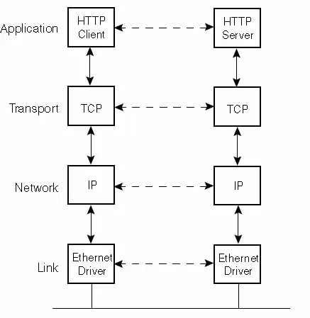
2.2.4 Encapsulation
When an application transmits data via TCP, the data traverses the protocol stack, progressing through each layer until it transforms into a stream of bits transmitted across the network. At each layer, headers are prepended, and trailers are added to the received data, as illustrated in Figure 2.17.
Here are some key abbreviations:
– TCP segment: The data unit sent by TCP to IP.
– IP datagram: The data unit sent by IP to the network interface.
– Frame: The flow of bits moving across the Ethernet.
IP (Internet Protocol) appends an identifier to the IP header it generates to specify the data’s layer. This is achieved by incorporating an 8-bit value, known as the protocol field, within its header. Likewise, multiple applications may concurrently utilize TCP or UDP. The Transport Layer protocol includes an identifier in the header it generates to discern the application. TCP and UDP both utilize 16-bit port numbers for application identification.
The source port number and destination port number are stored in the headers of TCP and UDP. Frames are sent and received by the network interface on behalf of IP, ARP, and RARP. The Ethernet header includes a 16-bit frame type field to identify the network layer protocol generating the data.
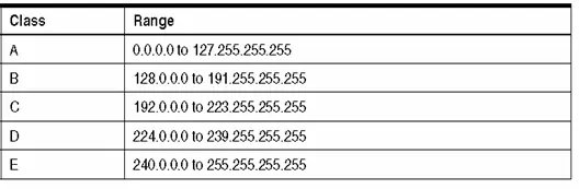
2.2.5 Internet Addresses
Each internet interface is assigned a distinct Internet Address, commonly known as an IP Address, which is represented as a 32-bit numerical value. Figure 2.18 illustrates the configuration and the five distinct classes of Internet addresses.
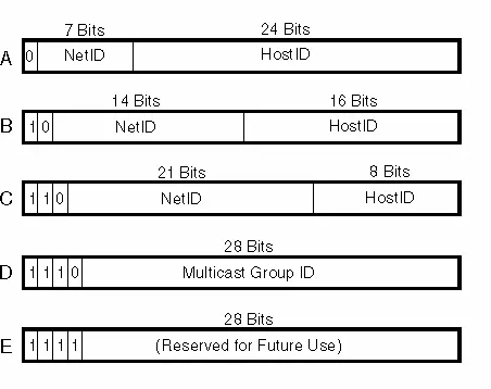
The standard representation for 32-bit addresses involves expressing them as four decimal numbers, with each number corresponding to a byte of the address. This format is commonly referred to as dotted-decimal. Given that each internet interface requires a distinct IP address, a central authority is necessary to allocate these addresses for networks linked to the global Internet. The Internet Network Information Center (NIC) serves as the responsible authority for this allocation. The dotted decimal notation for IP address classes is provided in Table 3.
2.2.6 IP (Internet Protocol)
IP datagrams carry all TCP, UDP, and ICMP data during transmission. IP offers an unreliable and connectionless delivery service for datagrams, with no assurance of successful delivery to the destination. In the event of an issue, IP employs a straightforward error-handling algorithm, discarding the datagram and attempting to send an ICMP message back to the source. Reliability, if needed, must be ensured by the upper layers of the communication protocol.
2.2.6.1 IP Header
In Figure 2.19, the structure of an IP datagram is depicted. The standard size of the IP header is typically 20 bytes, with variations if options are included. The leftmost bit is denoted as bit 0, while the rightmost bit of a 32-bit value is labeled as bit 31. The 32-bit value’s 4 bytes are transmitted in the sequence: bits 0 – 7, followed by bits 8 – 15, and so forth. This arrangement, known as Big-Endian byte ordering, is essential for all binary integers within TCP/IP headers as they traverse a network, and it is referred to as the network byte order.
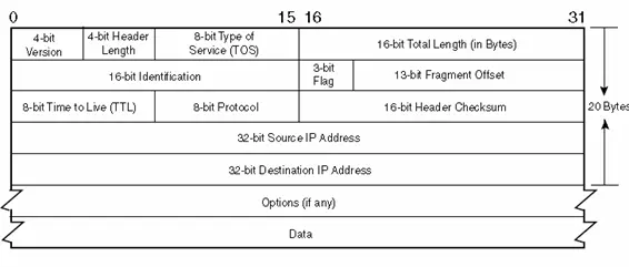
Header length:
The header length is determined by the count of 32-bit words (equivalent to 4 bytes per word) within the header, encompassing any options. This constraint confines the header length to 60 bytes.
Type of Service (TOS):
The Type of Service (TOS) field consists of a 32-bit precedence field (currently disregarded), 4 TOS bits, and an unused bit that should be set to 0. The 4 TOS bits represent options: minimize delay, maximize throughput, maximize reliability, and minimize monetary cost. Only one of these bits can be activated at a time. If all 4 bits are set to 0, it indicates normal service.
Total Length:
This represents the overall size of the IP datagram measured in bytes. By leveraging this field along with the header length field, we can determine the starting point and length of the data segment within the IP datagram. As this field is 16 bits, the IP datagram’s maximum size is 65535 bytes.
Identification:
Each datagram sent by a host is distinguished by this field, which typically increases by one with each transmission.
Time To Live:
The time-to-live (TTL) feature establishes a maximum threshold for the number of routers a datagram can traverse, thereby restricting the lifespan of the datagram. The sender initializes this value to a specific amount (commonly 32 or 64), and it decreases by one at each router that processes the datagram. When this TTL field reaches zero, the datagram is discarded, and the sender receives notification through an ICMP message. This mechanism safeguards against the possibility of the packet being trapped in endless routing loops.
Protocol:
The protocol is employed by IP to demultiplex incoming datagrams, determining the specific protocol that provided the data for transmission by IP.
Header Checksum :
The Header checksum is computed solely over the IP header, excluding any subsequent data. ICMP, UDP, and TCP each have their own checksum in their headers, encompassing both their header and data. Each IP datagram includes 32-bit values for the source IP address and the destination IP address.
The Option Field:
This comprises an assortment of optional data for datagrams, with a variable length. The utilization of these options is infrequent, and not all hosts and routers are equipped to support them.
2.2.7 TCP (Transmission Control Protocol)
TCP and UDP operate within the same network layer (IP), but they offer distinct services to the Application Layer. TCP, in particular, delivers a connection-oriented, reliable, byte-stream service. The term “connection-oriented” implies that before data exchange can occur, the two applications utilizing TCP must establish a connection with each other.
TCP ensures reliability through the following mechanisms:
– Application data is divided into optimal-sized chunks, referred to as segments, before transmission. This contrasts with UDP, where each application write generates a UDP datagram of corresponding size.
– Upon sending a segment, TCP initiates a timer, awaiting acknowledgment from the receiving end. In the absence of timely acknowledgment, the segment undergoes retransmission.
– When TCP receives data from the other end, it sends an acknowledgment, typically delayed by a fraction of a second.
– TCP applies an end-to-end checksum to its data header, detecting any alterations during transit. If a segment arrives with an invalid checksum, TCP discards it without acknowledgment, prompting the sender to retransmit after a timeout.
– As TCP segments are transmitted as IP datagrams, and IP datagrams can arrive out of order, TCP handles the resequencing of data, ensuring proper order before passing it to the application.
– To account for potential duplications in IP datagrams, receiving TCP must discard duplicate data.
– TCP incorporates flow control by allocating a finite buffer space to each end of the connection. A receiving TCP restricts the sender from transmitting more data than the available buffer can accommodate, preventing a fast host from overwhelming a slower one.
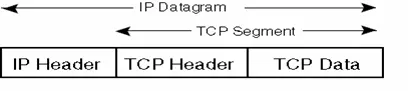
TCP data is encapsulated in an IP datagram, as illustrated in Figure 2.20.
2.2.7.1 TCP Header
The structure of the TCP header is depicted in Figure 2.21. Typically, it consists of 20 bytes, but this size may vary if options are included.
Sequence Number:
This indicates the sequential flow of bytes from the sending TCP to the receiving TCP, with the first byte of data in the segment representing a specific position in this sequence. TCP assigns a unique sequence number to each byte, utilizing a 32-bit unsigned number that resets to 0 after reaching 2^32-1.
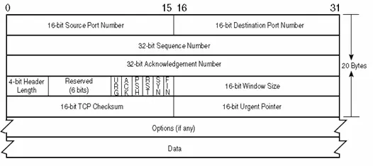
Acknowledge Number:
It includes the succeeding sequence number anticipated by the acknowledgment sender. Consequently, this number is the sequence number of the last successfully received byte of data plus 1. This field holds significance only when the ACK flag is activated. The 32-bit acknowledgment number is a consistent component of the header, accompanied by the always-set ACK flag.
Header Length:
This specifies the header length in terms of 32-bit words, a necessity due to the variable size of the options field. The presence of a 4-bit field restricts TCP to a maximum header size of 60 bytes. Conversely, in the absence of options, the standard header size reduces to 20 bytes.
- What microcontroller is used for the embedded web server?
The ATmega32 8-bit AVR microcontroller is used for its throughput and SPI capability. - Which Ethernet controller interfaces with the ATmega32?
The ENC28J60 Ethernet controller is used and interfaces via SPI. - How does the ENC28J60 connect to the network physically?
It connects through an RJ-45 connector using 10BASE-T twisted-pair cabling; an Integrated Magnetics RJ-45 Jack can be used. - Can an 8-bit microcontroller host a small web page?
Yes; the ATmega32 with 32 KB Flash can store a small web page for the embedded web server. - What voltage regulators are used for power supplies?
LM7805 is used to provide 5V for the ATmega32 and LM317 is used to provide 3.3V for the ENC28J60. - How many SPI lines are required between ATmega32 and ENC28J60?
Five lines are sufficient for the interface, typically including MISO, MOSI, SCK, SS, and an interrupt line. - What feature of the MagJack avoids using a crossover cable?
The AutoMDIX feature automatically swaps Tx and Rx as needed so a straight cable can be used. - What network protocols should be understood before programming the ATmega32?
TCP/IP protocol suite topics including Ethernet frame structure, IP, TCP, UDP, and HTTP should be understood. - How does the ENC28J60 notify the microcontroller of received packets?
It triggers an interrupt to the microcontroller when a data packet is received. - What interface standard does the ENC28J60 comply with?
The ENC28J60 is compliant with IEEE 802.3 Ethernet standards and integrates MAC and 10BASE-T PHY.