Summary of DIY Etching of Printed Circuit Boards (PCB)
DIY PCB creation via UV exposure and etching enables rapid, low-cost custom circuit board fabrication with high quality. This method involves designing layouts, transferring them to copper blanks using UV light, developing with Sodium Hydroxide, etching with Ferric Chloride, drilling, and screen printing. It is ideal for hobbyists avoiding professional manufacturing costs while achieving precise results.
Parts used in the DIY PCB Project:
- Circuit Board Design Software
- UV sensitive PCB board Blanks
- UV light source
- Personal Protection Equipment
- Sodium Hydroxide Solution
- Ferric Chloride
- Running wash water
- Shallow plastic trays
- Wood or plastic tongs
Making your own PCB boards for DIY electronics projects is not difficult. Doing so as a DIY project is extremely handy and allows almost anyone to custom design one-off, or small batch circuit layouts relatively quickly and cheaply, without the need for the volumes or costs involved in using the services of professional circuit board manufacturers. With care, DIY PCB project results are usually of extremely high quality and are very satisfying. Even more interest can be added to projects when printed circuit boards are combined with CNC cutter designs for shaping of the circuit boards.
There are various different methods for making PCB boards. Each method has various pros and cons, with most considerations being linked to cost, quality of finished product, accuracy required for fine circuits and availability of chemicals and materials.
Here we describe the UV exposure method for transfer of circuit layout image to a pre-sensitized Copper coated PCB blank, followed by etching with Ferric Chloride. The technique is accurate, convenient and provides a high quality etching.
Basic Outline of Steps Required
The UV exposure and etching method requires 6 main steps:
- Design and print the circuit layout onto transparency
- Transfer the circuit design onto a Copper coated PCB blank using UV light exposure
- Develop the exposed image using Sodium Hydroxide
- Etch away Copper between the required circuit tracks and contacts
- Drill holes in the PCB for placement of components (for through-hole PCB designs)
- Screen print and protect the PCB
Required Materials
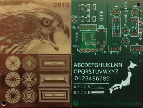
In the past, perhaps the biggest hindrance in using the UV exposure method was perhaps the availability of the required UV sensitized PCB blanks. However, these days, the copper coated PCB blanks and all other chemicals and materials are readily available online or from any good chemical or electronics supply outlet. Our preferred brand and supplier for many electronics and circuit board materials, from Japan is Sunhayato.
- (Optional) Circuit Board Design Software to produce layout design
- UV sensitive PCB board Blanks
- UV light source (UV lamp, tungsten element spot light, or in a pinch, bright sunshine)
- Personal Protection Equipment (chemical resistant gloves, eye goggles, chemical resistant apron, etc)
- Sodium Hydroxide Solution for developing – ie: highly corrosive!
- Ferric Chloride (for Copper etching) – ie: also highly corrosive and toxic!
- Ample running wash water
- Shallow plastic trays (x2) nb: Do not use metal!
- Wood or plastic tongs
Computer Design Software Available
Computer circuit and PCB design packages with Opensource GPL, free or sponsored licenses will more than likely satisfy the needs of many DIY electronics hobbyists. Some examples include: Fritzing, PCB Artist, DipTrace, XCircuit and gEDA to name a few. These are listed without order or preference and offer differing features, capability and quality.
Many commercial design packages are also available, but can be pricy if you are just messing with home DIY projects. Such an option that we like however is Eagle PCB by CadSoft, which offers a non-profit, DIY hobbyist license of Eagle PCB (free at time of writing) if you are able to truthfully sign and comply with their non-profit declaration.
For more detail: DIY Etching of Printed Circuit Boards (PCB)
- What are the main steps required for the UV exposure method?
The process requires six main steps: design and print layout, transfer design via UV light, develop image, etch copper, drill holes, and screen print. - Can I use metal trays for the development and etching stages?
No, you must not use metal; only shallow plastic trays should be used. - Which chemicals are used for developing and etching?
Sodium Hydroxide is used for developing, and Ferric Chloride is used for etching away the copper. - Is personal protection equipment necessary during this project?
Yes, you need chemical resistant gloves, eye goggles, and a chemical resistant apron due to corrosive materials. - Where can I obtain UV sensitive PCB board blanks?
These blanks are readily available online or at good chemical and electronics supply outlets. - Does the article recommend any specific free design software?
Yes, examples include Fritzing, PCB Artist, DipTrace, XCircuit, gEDA, and Eagle PCB for non-profit users. - What tools are needed to handle chemicals safely?
Wood or plastic tongs are required to handle items in the chemical trays. - How does the cost of DIY PCBs compare to professional services?
DIY projects allow for quick, cheap one-off or small batch designs without the volumes or costs of professional manufacturers.