
Summary of EFABLESS LAUNCHES CHIPIGNITE WITH SKYWATER TO BRING CHIP CREATION TO THE MASSES
Efabless launched the chipIgnite program to democratize chip design by offering low-cost fabrication via SkyWater's open-source SKY130 process. This initiative removes barriers by providing pre-designed carrier chips, automated design flows, and reference templates, enabling users to create and test chips without deep semiconductor expertise or high costs.
Parts used in the chipIgnite:
- Pre-designed carrier chip
- Automated open source design flow
- SkyWater SKY130 process node
- Development board
- Firmware stack
- Full chip reference design template
- Physical IO implementation
- Common management area
- SkyWater Open Source PDK
- Program includes a pre-designed carrier chip and automated open source design flow from Efabless
- SkyWater’s open source SKY130 process is the first node to be used to fabricate chips for the program
- Initiative removes access barriers by significantly reducing cost and the need for deep semiconductor experience to design chips
Efabless, a community chip creation platform, today announced the launch of its new chipIgnite program to bring chip design and fabrication to the masses and collaboration with SkyWater Technology for the first node supported in the program. The chipIgnite program expands upon the SKY130-based open-source chip manufacturing program sponsored by Google and supports private commercial designs that include non-open source IP. This initiative represents another step forward in the industry to broaden access to chip design by giving people the ability to more easily create and fabricate chips.
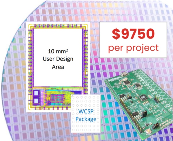
The chipIgnite program offers unique value to the designer which includes not only low-cost manufacturing but also a development board and firmware stack to simplify design validation and test. All projects created as part of the chipIgnite program will utilize a full chip reference design template that implements the physical IO for the chip as well as provides a common management area to support the test and evaluation of the user’s design. The program also includes an optional automated open-source design flow for implementing projects that enable users to generate layouts for their digital projects from RTL. The chipIgnite program will provide users a guaranteed reservation to ensure their project is included.
SkyWater’s open-source 130 nm CMOS platform will be used to fabricate chips for the chipIgnite program. The automotive-grade mixed-signal platform is well suited for IoT and edge computing as it is in a sweet spot for enabling a combination of both digital and analog circuit performance with embedded non-volatile memory for a wide range of SoC architectures. The program provides users 10 mm2 of the total project area with fabrication for projects using the SkyWater Open Source PDK.
Read more: EFABLESS LAUNCHES CHIPIGNITE WITH SKYWATER TO BRING CHIP CREATION TO THE MASSES
-
What is the chipIgnite program?
It is a new initiative by Efabless designed to bring chip design and fabrication to the masses through collaboration with SkyWater Technology. -
Which process node supports the chipIgnite program?
The program uses SkyWater's open-source SKY130 process, which is the first node utilized for this specific initiative. -
How does the program reduce access barriers?
It significantly reduces cost and minimizes the need for deep semiconductor experience required to design chips. -
What value does the program offer designers?
It provides low-cost manufacturing along with a development board and firmware stack to simplify design validation and testing. -
Can private commercial designs use this program?
Yes, the program supports private commercial designs that include non-open source IP. -
What is included in the full chip reference design template?
The template implements physical IO for the chip and provides a common management area to support test and evaluation. -
Is there an automated design flow available?
An optional automated open-source design flow is included to enable users to generate layouts for digital projects from RTL. -
What project area is provided for fabrication?
The program provides users with 10 mm2 of total project area for fabrication using the SkyWater Open Source PDK.
