Summary of Exploring the Atmega32: A Comprehensive Guide to AVR Microcontrollers
ATmega32 and ATmega8 are 8-bit AVR microcontrollers using an enhanced RISC architecture with low power use, on-chip flash, SRAM, EEPROM, multiple timers, ADC, PWM, serial interfaces (USART, SPI, TWI), and several sleep modes. ATmega32 offers 32 KB flash, 2 KB SRAM, 1 KB EEPROM, 32 I/O lines, 8-channel 10-bit ADC, and multiple timers. ATmega8 provides 8 KB flash, 1 KB SRAM, 512 B EEPROM, 6-channel ADC, and internal RC oscillator options. Both support in-system programming, interrupts, brown-out detection, and various power-saving modes.
Parts used in the ATmega32 and ATmega8 Overview:
- ATmega32 microcontroller
- ATmega8 microcontroller
- VCC (digital supply)
- GND (ground reference)
- Port A (PA7-PA0) pins
- Port B (PB7-PB0) pins
- Port C (PC7-PC0) pins
- Port D (PD7-PD0) pins
- Reset pin
- XTAL1 pin (oscillator input)
- XTAL2 pin (oscillator output)
- AVCC pin (A/D converter supply)
- AREF pin (A/D reference)
- Crystal or external oscillator (optional)
- Bootloader/boot program (on-chip)
- In-system programming interface (AVR dude/toolchain)
- ADC channels (ATmega32: 8-channel, ATmega8: 6-channel)
- Timers/Counters (two 8-bit, one 16-bit)
- USART serial interface
- SPI serial interface
- TWI (Two-Wire Interface) on ATmega8
- Watchdog timer (with on-chip oscillator)
- EEPROM memory (ATmega32: 1024 bytes, ATmega8: 512 bytes)
- SRAM (ATmega32: 2 KB, ATmega8: 1 KB)
- Flash program memory (ATmega32: 32 KB, ATmega8: 8 KB)
ATmega32 – 8 Bit AVR Microcontroller
Key Features:
• 32 kilobytes of flash program memory that is in-system self-programmable.
• 2 kilobytes of internal SRAM (Static Random-Access Memory).
• 1024 bytes of EEPROM (Electrically Erasable Programmable Read-Only Memory).
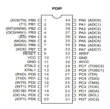
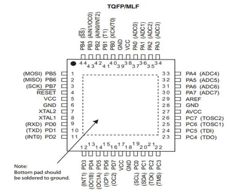
• Available in 40-pin DIP (Dual Inline Package), 44-lead QTFP (Quad Flat Thin Package), and 44-pad QFN/MLF (Quad Flat No-Lead/Micro Lead Frame).
• 32 programmable I/O (Input/Output) lines for versatile connectivity.
• 8-channel, 10-bit ADC (Analog-to-Digital Converter) for precise analog signal conversion.
• Two 8-bit timers/counters featuring separate prescalers and compare modes.
• One 16-bit timer/counter with a separate prescaler, compare mode, and capture mode.
• 4 PWM (Pulse Width Modulation) channels for effective motor and light control.
• In-system programming facilitated by an on-chip boot program.
• Programmable watchdog timer with a separate on-chip oscillator for enhanced system reliability.
• Programmable serial USART (Universal Synchronous/Asynchronous Receiver/Transmitter) for serial communication.
• Master/slave SPI (Serial Peripheral Interface) serial interface for efficient data exchange.
Special Microcontroller Features:
• Utilizes an internal calibrated RC oscillator for precise timing.
• Supports both external and internal interrupt sources for flexible event triggering.
• Incorporates power-on reset functionality and programmable brown-out detection for enhanced system reliability.
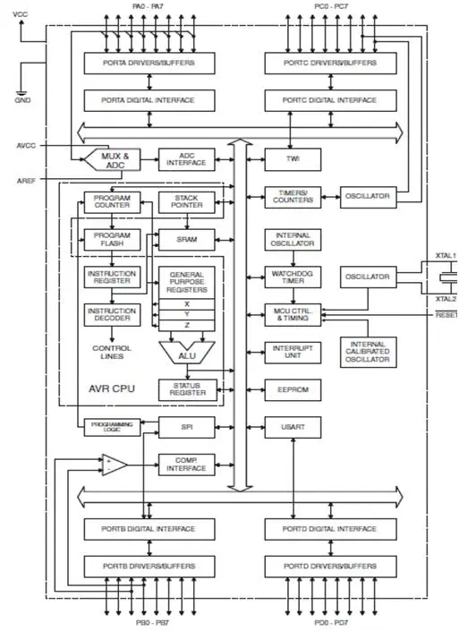
All 32 registers are directly linked to the Arithmetic Logic Unit (ALU), enabling the access of two independent registers in a single instruction executed within a single clock cycle. During power-down, the register contents are preserved, but the oscillator is halted, resulting in the deactivation of all other chip functions until an external interrupt occurs. The asynchronous timer permits the maintenance of a timer-based power-save mode while the remainder of the device remains in a sleep state.
In ADC noise reduction mode, the CPU and all I/O modules, except ADC and the asynchronous timer, are halted. In standby mode, the entire device, with the exception of the crystal oscillator, enters a sleep state. Extended standby mode ensures that both the main oscillator and asynchronous timer continue to operate.
The ATmega32 stands out as a robust microcontroller due to its in-system self-programmable flash integrated on a monolithic chip. This feature provides a highly flexible and cost-effective solution for a variety of embedded control applications.
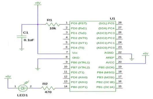
Pin Descriptions:
VCC:
Supply of digital voltage
GND:
Reference to the ground
Port A (PA7-PA0):
This port functions as analog inputs for the A/D converter and operates as an 8-bit bidirectional I/O port in the absence of A/D converter usage.
Port B (PB7-PB0) & Port D (PD7-PD0):
These are 8-bit bidirectional I/O ports with symmetrical drive characteristics in their output buffers, offering both high sink and source capabilities. When configured as inputs, they are significantly pulled low when pull-up resistors are engaged. Additionally, these ports serve various special function features of the ATmega32.
Port C (PC7-PC0):
An 8-bit bidirectional I/O port where, if the JTAG interface is enabled, the pull-up resistors on pins PC5 (TDI), PC3 (TMS), and PC2 (TCK) will be activated.
Reset:
– An input signal that initiates a system reset.
XTAL1:
– Serves as both an input to the inverting oscillator amplifier and as an input to the internal clock operating circuit.
XTAL2:
– Outputs from the inverting oscillator amplifier, contributing to the external clock signal.
AVCC:
– The supply voltage pin specifically designated for Port A and the A/D converter. It must be connected to VCC.
AREF:
– AREF functions as the analog reference pin for the A/D converter.
ATmega32 Memories:
– This microcontroller features two primary memory spaces: data memory and program memory space. Additionally, it includes EEPROM memory for persistent data storage.
In-System Programmable Flash Program Memory:
– ATmega32 incorporates 32 kilobytes of on-chip in-system reprogrammable flash memory for program storage. The flash memory is organized as 16k x 16 and is divided into two sections: the Boot program section and the application program section.
SRAM Data Memory:
The lower 2144 data memory locations encompass the addressing of the Register file, I/O memory, and internal data SRAM. The initial 96 locations target the Register file and I/O memory, while the subsequent 2048 locations are dedicated to addressing the internal data SRAM. There are five distinct addressing modes for data memory coverage: direct, indirect with displacement, indirect, indirect with pre-decrement, and indirect with post-decrement. Utilizing these addressing modes allows access to the 32 general-purpose registers, 64 I/O registers, and 2048 bytes of internal data SRAM.
EEPROM Data Memory:
It encompasses a data EEPROM memory of 1024 bytes, accessible as a distinct data space for individual byte reading and writing.
I/O Memory:
All input/output operations and peripherals are situated within the I/O space. The IN and OUT instructions are employed to transfer data between the 32 general-purpose registers and the I/O space. I/O registers within the address range 00-1F are directly manipulated at the bit level using the SBI and CBI instructions.
Introduction to ATmega8:
The ATmega8 belongs to the AVR family, a 8-bit CMOS microcontroller developed by Atmel Corporation in 1996. It operates on the RSIC (Reduced Instruction Set Computer) architecture. One of its key advantages lies in the absence of an accumulator, allowing the result of any operation to be stored in a register defined by the instruction.
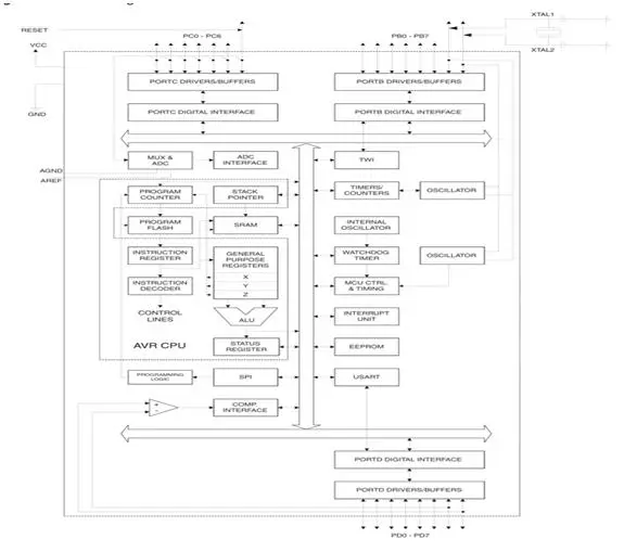
Memory
It is equipped with 8 kilobytes of flash memory, 1 kilobyte of SRAM, and 512 bytes of EEPROM. The 8K flash is divided into two sections – the lower part functions as the boot flash section, while the upper part serves as the application flash section. Within the SRAM, there are 1 kilobyte along with 1120 bytes allocated for general-purpose registers and I/O registers. The lower 32 address locations are dedicated to 32 general-purpose 8-bit registers, while the subsequent 64 addresses are assigned to I/O registers, all directly linked to the Arithmetic Logic Unit (ALU). The EEPROM is utilized for storing user-defined data.
In terms of input/output ports, the configuration includes 23 I/O lines distributed across three ports, namely B, C, and D. Port B encompasses 8 I/O lines, Port C comprises 7 I/O lines, and Port D consists of 8 I/O lines. The registers corresponding to any port X (B, C, or D) are as follows: DDRX (Port X data direction register), PORTX (Port X data register), and PINX (Port X input register).
The device also features three timers with comparable modes, including two 8-bit timers and one 16-bit timer.
Oscillators
Communication
It offers both synchronous and asynchronous data transfer options through the Universal Synchronous and Asynchronous Receiver Transmitter (USART), enabling communication with modems and various serial devices. Additionally, it supports the Serial Peripheral Interface (SPI) for communication between devices using the master-slave method. Another supported communication type is the Two-Wire Interface (TWI), facilitating communication between two devices through 2 wires and a common ground connection.
The chip integrates a comparator module that enables voltage comparison between two inputs connected to external chips. Furthermore, it features a 6-channel Analog-to-Digital Converter (ADC), with 4 channels providing 10-bit accuracy and 2 channels offering 8-bit accuracy.
Status Register: This register contains information about the currently executed arithmetic instruction set.
ATmega Pin Diagram:
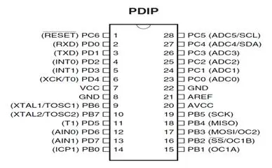
One notable feature of the ATmega8 is that, with the exception of 5 pins, all other pins support two signals.
For port assignments, pins 23, 24, 25, 26, 27, 28, and 1 are designated for port C, while pins 9, 10, 14, 15, 16, 17, 18, and 19 are allocated for port B, and pins 2, 3, 4, 5, 6, 11, and 12 serve port D.
Pin 1 functions as the Reset pin, triggering a reset if a low-level signal is applied for a duration longer than the minimum pulse length.
Pins 2 and 3 are employed for serial communication in USART, while pins 4 and 5 serve as external interrupts. One triggers when the interrupt flag bit of the status register is set, and the other triggers as long as the interrupt condition persists.
Pins 9 and 10 function as external oscillators and timer counters oscillators, where pin 10 can be used for a crystal oscillator or low-frequency crystal oscillator. Additionally, when the internal calibrated RC oscillator is the clock source and the asynchronous timer is enabled, these pins can serve as timer oscillator pins.
Pin 19 serves as the Master Clock output and slave clock input for the SPI channel, while pin 18 is used as the Master clock input and slave clock output.
Pin 17 is designated as Master data output and slave data input for the SPI channel, functioning as an input when enabled by a slave and bidirectional when enabled by the master. This pin can also serve as an output compare match output, acting as an external output for the timer/counter compare match.
Pin 16 serves as a slave select input and can also be configured as a timer/counter1 compare match by setting PB2 as an output.
Pin 15 can be utilized as an external output for the timer/counter compare match A.
Pins 23 to 28 are assigned for ADC channels, with pin 27 also potentially serving as the Serial Interface Clock and pin 28 as the Serial Interface Data.
Pins 13 and 12 are designated as Analog Comparator inputs, while pins 11 and 6 are utilized as timer/counter sources.
Microcontroller Sleep Modes
The microcontroller features six sleep modes, each serving distinct purposes.
1. Idle Mode:
– This mode halts the CPU’s operation while allowing the SPI, USART, ADC, TWI, Timer/Counter, and Watchdog, as well as the interrupt system, to function.
– Activation involves setting the SM0 to SM2 bits of the MCU register flag to zero.
2. ADC Noise Reduction Mode:
– This mode stops the CPU while permitting the operation of the ADC, external interrupts, Timer/Counter2, and the watchdog.
3. Power Down Mode:
– External interrupts, the 2-wire serial interface, and the watchdog are enabled in this mode, while the external oscillator is disabled, leading to the cessation of all generated clocks.
4. Power Save Mode:
– Employed when the Timer/Counter is clocked asynchronously, this mode halts all clocks except clk
ASY.
5. Standby Mode:
– In Standby mode, the oscillator continues to operate, while all other operations come to a halt.
Applications Involving Atmega8
- What is the flash memory size of the ATmega32?
ATmega32 has 32 kilobytes of in-system self-programmable flash program memory. - How much SRAM does the ATmega8 provide?
ATmega8 provides 1 kilobyte of SRAM. - Can the ATmega32 perform in-system programming?
Yes, ATmega32 includes an on-chip boot program for in-system self-programmable flash. - What ADC channels are available on the ATmega32?
ATmega32 has an 8-channel, 10-bit ADC. - Does the ATmega8 include an internal RC oscillator?
Yes, the ATmega8 has an internal RC oscillator with selectable frequencies (1MHz, 2MHz, 4MHz, 8MHz). - What sleep modes do these microcontrollers support?
They support six sleep modes: Idle, ADC noise reduction, Power-save, Power-down, Standby, and Extended standby. - How is EEPROM accessed on the ATmega32?
ATmega32 has 1024 bytes of EEPROM accessible as a separate data space for byte read and write. - What serial interfaces do ATmega32 and ATmega8 support?
Both support USART and SPI; ATmega8 also supports TWI (Two-Wire Interface). - Which pins are used for XTAL and oscillator functions?
XTAL1 is the input to the inverting oscillator amplifier and clock circuit; XTAL2 is the output from the inverting oscillator amplifier. - How is a simple blinking LED program delivered to the microcontroller?
The C source is compiled to an ELF file, converted to a hex file, and uploaded to the microcontroller using the AVR dude program.