Summary of I2C Bus for ATtiny and ATmega
This article introduces the use of the I2C (Inter-Integrated Circuit) bus to expand the input/output capabilities of Atmel AVR microcontrollers like the ATtiny2313 and ATmega168. It explains how the two-wire I2C interface allows multiple peripherals (such as I/O expanders, SRAM, and EEPROM) to connect using only two microcontroller pins, overcoming the limitation of limited I/O lines. The article discusses the hardware differences between the microcontrollers, I2C addressing, and practical tips for implementing and using I2C with AVRs, accompanied by example devices and part numbers for experimentation.
Parts used in the I2C Bus for ATtiny and ATmega Project:
- ATtiny2313 microcontroller
- ATmega168 microcontroller
- PCA8574A I2C I/O Expander
- PCA8574 I2C I/O Expander
- 24C16 EEPROM (CAT24C16LI-G)
- 256x8 SRAM with I2C interface
- Pull-up resistors (typically 1.8K to 10K, recommended 5.1K)
I love the Atmel AVR microcontrollers! Since building the Ghetto Development System described in this Instructable. I’ve had no end of fun experimenting with the AVR ATtiny2313 and the ATmega168 in particular. I even went so far as to write an Instructable on using switches as inputs, and extended the Ghetto Development System concept to CPLDs.
During a recent project, I needed several switches for setting control values. The AVRs did not have enough I/O pins, so I had to think of something. I could have tried a complex input system with a keyboard and display, but the ATtiny2313 would have run out of resources. Fortunately, Atmel has provided a way around this problem by including an interface that can link to additional chips (such as memory or I/O ports) with a simple two wire interface. That’s right, by using just two I/O pins on an AVR we can access many additional I/O pins, and other resources as well.
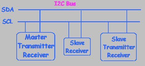
This two wire interface is formally known as the Inter-Integrated Circuit bus, or just the I2C bus and was invented by NXP when it was still Philips Semiconductors. If you’re reading this Instructable then you’ve probably heard of the I2C bus and may even have used it on a PIC or other microcontroller. While conceptually very simple, and supported by hardware resources on the AVRs, software drivers are still necessary to use the I2C bus. Atmel provides Application Notes (see the Resources later in this Instructable), but these are incomplete and don’t show any examples beyond communicating with another AVR device.
It is not the purpose of this Instructable to teach anyone how to create I2C drivers for the AVRs. Rather, I’ll provide expanded versions of the Atmel drivers for ATtiny2313 and ATmega168 devices, I’ll explain the requirements and restrictions that apply when using these, and I’ll show you working examples of I2C devices. After you work through this Instructable you’ll be able to use the I2C bus successfully in your AVR projects. Obviously, you can ignore the drivers for either tiny or MEGA if you’re only interested in one of them. For those interested in learning more about the I2C bus, I’ll provide links to appropriate material.
Step 1: What’s All this I2C stuff anyway?
The electrical requirements are pretty simple. The master and the slaves must use the same level for Vcc, the grounds must be connected, and the SCL and SDA lines must be pulled up to Vcc. The value of the pull-up resistors is precisely determined by a calculation based on the total capacitance on the bus, but practically can be pretty much any value between 1.8K and 10K. I start with 5.1K and use lower values until it works. This usually isn’t an issue unless you have a lot of devices or long lengths of wire between devices.
The nominal data rate on the I2C bus is 100Kbits/second. Rates of 400Kbits/second, 1Mbits/second, and beyond are possible as well, but aren’t supported by the drivers in this Instructable. All I2C devices will work at 100Kbits/second.
The ATtiny2313 and the ATmega168 each implement the I2C bus differently. ATtiny2313 uses the Universal Serial Interface (USI) hardware – which can also be used for the SPI bus. ATmega168 has dedicated hardware for the I2C bus known as the Two Wire Interface (TWI). Once the drivers are written, these differences are mostly transparent to the user. One significant difference is in the software: The ATmega168 I2C driver is interrupt driven while that for the ATtiny2313 is not. This means that an ATmega168 program does not have to wait for I2C data transfers to take place, but only needs to wait before initiating another transfer, or until data arrives from a read operation. The examples and discussion to follow should make this clear.
I2C addresses are 7 bits long, so up to 127 devices can be on the bus if each has a unique address. As shown in the figure, this 7 bit address is shifted left one bit and the least significant bit is used to flag a read or write of the device at the address. Thus the complete slave address is an 8 bit byte. The actual address is partially determined internally to the device and can’t be changed (4 most significant bits), and partially determined by bits that may be connected to device pins (3 least significant bits) that can be tied high or low to set a specific address.
Sounds confusing, but an example will make this clear. The PCA8574A data sheet shows that the four most significant bits of the I2C address will always be 0111. The next three bits are determined by the settings on pins AD0, AD1 and AD2. These pins can be tied to ground or to the positive voltage supply (5 volts) to represent 0 or 1 respectively. So the range of possible addresses is 38 to 3F hexadecimal, as shown in the other figure from the PCA8574 data sheet.

Determining the address of a given device can be confusing since some data sheets consider the read/write bit to be part of the address. Read the data sheet carefully and keep in mind that the slave address will be 7 bits long. The read/write bit should be treated separately. Again, an example will help. The data sheet for the 24C16 EEPROM we’ll experiment with says the first (most significant) four bits of the slave address are 1010. The next three bits can be determined by A0, A1 and A2. But note the data sheet also covers 24C01 through 24C08 which are smaller sized EEPROMs. The figure from the data sheet shows that the settings of these address bits are ignored as the size increases and are completely ignored for the 24C16. That is, the last three bits don’t matter and the 24C16 really uses all I2C slave addresses 50 through 57 hexadecimal. The range of slave addresses will actually address different sections within the 24C16. The first 256 bytes are at address 50h, the next 256 at 51h, and so on up to the last 256 at 57h – for a total of 2K bytes. Since the address of the PCF8570 RAM we also experiment with is in this range. The 24C16 and the PCF8570 can’t be used together.
Step 2: Order some I2C devices
Now that you know a little about the I2C Bus and want to use it, why not order some I2C devices to experiment with now so they can be on the way to you while you’re getting the software ready?
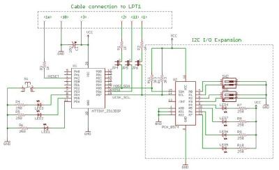
Appropriate devices include an I/O Interface Expander (my favorite), a Static Ram, and an EEPROM. There’s lots more, but these are a great start. The AVR processors we’ll use are the ATtiny2313 and the Atmega168 (used in Arduino). If you’re new to these, then have a look at this great Instructable to learn about them and build your Ghetto Development System. The schematic of the ATmega168 in the present Instructable shows how to implement the Ghetto Development System for this processor. The parallel port cable is the same as the one for the ATtiny2313. (I haven’t tried the USB version of the Ghetto Development System. So I’m not sure how the I2C bus is accessed on it. Same for the Arduino.)
Here are Digikey part numbers.
Port Expander:
IC I2C I/O EXPANDER 568-4236-5-ND
Ram:
IC SRAM 256X8 W/I2C 568-1071-5-ND
EEPROM :
IC EEPROM SERIAL 16K CAT24C16LI-G-ND
For more detail: I2C Bus for ATtiny and ATmega

