Summary of Step-by-Step Guide to PCB Layout Design with Proteus
Proteus is a PCB design and simulation suite combining ISIS (schematic capture/SPICE) and ARES (PCB layout). The article walks through creating a 38 kHz 555-timer circuit in Proteus, selecting components, simulating, exporting to ARES, drawing board edges, placing components, routing tracks (manual or auto-router), using layers and vias, 3D visualization, printing artwork/silk/resist/drill layers (mirror bottom copper), and fabricating the PCB via toner transfer, etching with ferric chloride, drilling, soldering, and finishing.
Parts used in the 38 kHz Frequency Generator Project:
- 555 timer IC
- 470 ohm resistor
- 22 kiloohm resistor
- 10 kiloohm variable resistor (potentiometer)
- 0.001 µF capacitor
- IR LED
- Proteus Design Suite software (ISIS and ARES)
- Copper-clad PCB board
- Printer and transfer paper
- Heat source (iron)
- Ferric chloride etchant
- Sandpaper
- Drill (for PCB holes)
- Soldering kit
- Cutter (for trimming leads)
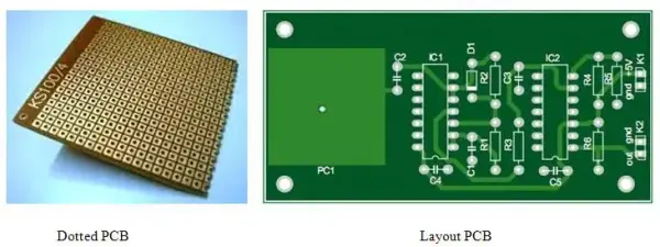
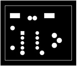
Frequently, terms like PCBs, PCB layout, and PCB design are commonly heard in electronic engineering discussions. However, what exactly is a PCB and why is it utilized? As electronic engineers, comprehending these concepts is crucial. PCB stands for Printed Circuit Board, which essentially refers to a circuit board featuring printed copper connections. PCBs are categorized into two types: one is the dotted PCB, while the other is the layout PCB. Below are examples illustrating both types.
So far, we’ve explored various types of PCBs and their distinctions. Now, let’s shift our focus to PCB design software. There exists a wide array of PCB design software options, including Express PCB, Eagle PCB, PCB Elegance, Free PCB, Open Circuit Design, Zenith PCB, and Proteus among others. Notably, Proteus stands out from the rest. It serves as a comprehensive design suite and PCB layout software. With Proteus, users can create and simulate circuits, subsequently generating a PCB layout tailored to the circuit’s specifications.
Introduction to Proteus:
Unleash your PCB design potential with Proteus Professional. This powerful software suite combines the intuitive ISIS schematic capture program with the ARES PCB layout program, creating an integrated development environment ideal for professionals and educators alike.
User-friendly tools guide you through every step of the design process, from sketching schematics and running SPICE simulations to creating professional-grade PCB layouts with ease.
Advanced features like auto-routing, highly configurable design rules, and 3D visualization empower you to bring your ideas to life. Industry-standard outputs ensure seamless integration with your existing workflows.
Whether you’re a seasoned professional or just starting out, Proteus Professional has the tools you need to take your PCB designs to the next level.

Following this, a workspace containing interface buttons for circuit design will be displayed, as depicted in the figure below. Please ensure that the entire circuit is created within the confines of the blue rectangular boundary within the workspace.

The subsequent stage involves choosing the components necessary for our desired circuit. To illustrate, consider the creation of a 38 kHz frequency generator utilizing a 555 timer IC. The circuit diagram is depicted in the image below.
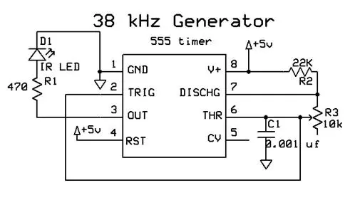
In the circuit provided, you’ll need the following components: a 555 timer IC, resistors of 470 ohms and 22 kilohms, a 10 kilohm variable resistor, a 0.001µF capacitor, and an IR LED. To select these components from the library, navigate to the menu bar and click on “library” > “pick device/symbol.” This action will open a window as described below.

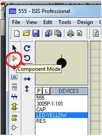
Another method exists for choosing the components. On the left side of the workspace, there’s a toolbar available. Within this toolbar, you can either click the component mode button or select from the library.
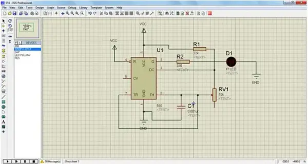
Choose all components available in the library and add them to the devices list. Next, select a device and adjust its angle using the rotate buttons. After adjusting, click on the workspace area, and the chosen component will be placed there. Continue placing all devices in the workspace, positioning the cursor at the end of each component’s pin, and draw connections using the pen symbol to interconnect all the components according to the circuit design. The resulting designed circuit will be displayed in the image below.
If you wish to make any changes to the component, simply hover the mouse cursor and right-click to reveal the options window, as depicted in the image below.

Once the design is finished, save it with a specific name and proceed to debug. This virtual simulation enables us to visualize the outcomes without physically constructing a circuit, allowing us to observe the results through software. Additionally, we can use this software to create the PCB layout for our desired circuit.
PCB Layout Designing
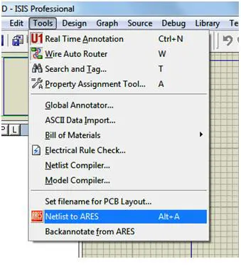
Now we are going to design a PCB layout for the above circuit. Proteus has the integrated ARES PCB designing suit. By using this we can easily develop the PCB layout. After simulation save the circuit designing and click on tools then select netlist to ARES. Then a window will open with list of component packages. That is shown in below image.

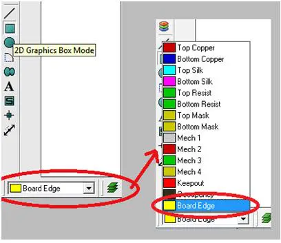
The subsequent action involves forming a board perimeter by choosing the 2D graphics box mode. Then, click on the layer selection located at the bottom left corner and opt for the board edge. The visual representation is depicted in the figure below.
- Click the “Work Space” button. A green line will appear.
- Draw a box around your desired PCB layout and click once to finish. The box will turn yellow and represent the design area. This is similar to the blue line box used in ISIS Professional.
- All components must be placed within the yellow box. If your circuit is large, you can expand the box by clicking “Select Mode” and then clicking and dragging the box edges.
- To rotate a component, select it and use the rotation arrow options provided.
- Place the component within the yellow box.
- After placing all components, arrange their positions as needed.
- Click “Select Mode” and click on a component to move it. The component will turn white. Hold and drag it to the desired location within the yellow box.
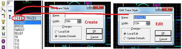
- To connect components with copper tracks, select “Track Mode.”
- Change the track width by clicking the “C” (create) or “E” (edit) buttons. A window will appear, allowing you to choose a width.
- For hobbyists making their own PCBs, I recommend a track width of 35. This will prevent potential cuts that may occur with thinner tracks.
The next step involves establishing connections between components. These connections are depicted by green and yellow lines indicating directionality. Once the track width is set, use a pen tool to start at one end of a component and follow the green line. Successful connection between two components results in the automatic removal of the green line.
Another important aspect concerns the different types of PCBs available. Single-layer PCBs have components on one side and tracking on the other side. Dual-layer PCBs involve tracking on both sides along with components placed on both sides, mostly utilizing SMD components. Moving to multi-layered PCBs, these boards consist of numerous layers. Typically, there are two outer layers (top and bottom) and several inner layers. In Proteus, the design allows for up to 16 layers of PCB. The layer selection in Proteus can be found in the bottom-left corner, with each layer represented by a different color. For instance, the bottom layer is shown in blue, the top layer in red, and the inner layers in various colors, as illustrated in the image below.

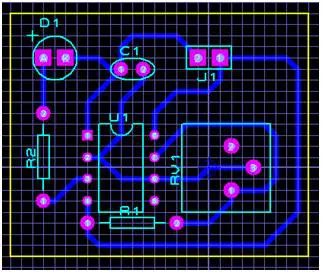
The image above illustrates the placement of a track between the R1-2 pin and RV1-1 pin. Additionally, a track is placed from the 6th pin to the 3rd pin, denoted by a directional white arrow. The connections are highlighted by green lines, while the tracks are represented by blue lines. Any contact errors during tracking are identified by red circles, as depicted in the subsequent figure below.
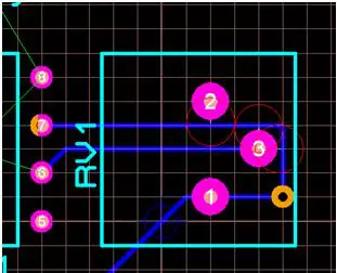
The circles depicted in red in the image above indicate tracking errors. To prevent these errors, adjust the track paths to ensure smooth connectivity between all pins. For those considering a dual-layer PCB, a convenient shortcut exists to switch between layers by quickly clicking the left mouse button twice, transitioning to the alternate layer. In the provided image, an orange circle signifies the use of a ‘via,’ facilitating connections between different layers. An advantage in Proteus lies in its auto-router feature—a specialized tool designed to automatically organize tracks, albeit typically generating dual-layer PCBs. Upon selecting this tool, a window named the shape-based auto-router opens, offering options to modify execution modes, design rules, and grid width. After customizing these settings as per requirements, initiating the auto-routing process can be done by clicking the ‘begin routing’ button.

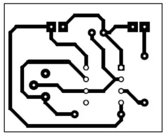
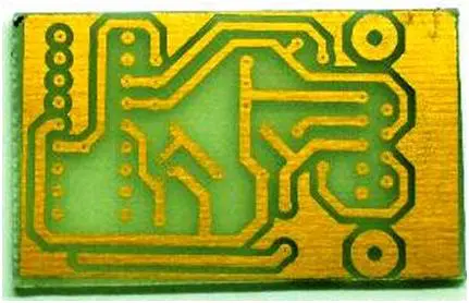
In the second image above, red tracks represent the top copper layer, while blue tracks represent the bottom layer. This signifies the design of a dual-layer PCB. For a single-layer PCB, we have the option to position tracks as needed. The image below displays the design of a single-layer PCB for our desired circuit. Once the tracking is finished, save the project in the same folder where the previous Proteus project was saved. In Proteus, there is another tool available that illustrates how the circuit will appear upon completion.
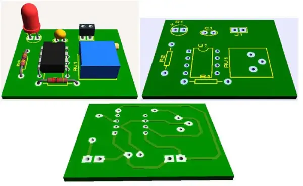
To view the completed circuit, access the menu bar and click on “Output,” then choose “3D Visualization.” This action will prompt a new window displaying the circuit visualization, featuring multiple angles, a board view with fewer components, and a view of the back layer, as illustrated in the figure below.
The last step in PCB layer designing involves printing the layout. To print the circuit layout, access the “Output” option in the menu bar and select “Print.” This action will prompt the print layout setup window to open.

Within that window, various options for layer selection, modes, paths, rotation, scaling, reflection, and image preview are accessible. As for the modes, there are four available: artwork, solder resist, SMT mask, and drill plot. The artwork mode displays our entire design, including tracks and component views, similar to the yellow-colored module view seen in the images above. When printing the bottom copper layer, a crucial consideration is the reflection selection, which should be set to mirror mode. This particular window’s layout is depicted in the figure below. Multiple prints of the circuit layout need to be obtained.
PCB Layout Printing
1. Printing the top copper layer is unnecessary for a single-layer PCB; this step is specifically for dual-layer PCBs.
2. Printing the bottom copper layer involves deselecting all boxes except for the bottom copper and board edge in the layers/artwork section. Then, set the scale to 100%, choose horizontal rotation for X, and importantly, select “mirror” for reflection. This mirror selection is crucial because when printing this layer onto paper, it will be placed on the copper board in the opposite direction. This ensures that the printed side faces the copper layer accurately.
The third step involves printing the top silk layer, which pairs with the bottom copper layer. In a single-layer PCB, only the bottom copper is utilized, leaving the components located on the top side. The top silk layer facilitates the printing of the component view, indicating their placement on the board. When printing this layer, all boxes except for the top silk and board edge must be deselected in the layers/artwork section. All other selections remain unchanged, except for the reflection option, which should be set to normal mode.
4. Printing the bottom silk layer, specifically designed for dual-layer PCBs.
5. Printing the solder resist layer is crucial to prevent short circuits. To print this layer, choose the solder resist mode. Click on the bottom resist box, encompassing both the board edge and the reflection mirror mode. This process mirrors the bottom copper layer printing procedure.
6. The SMT mark isn’t applicable here as our circuit doesn’t involve the use of SMT modules.
7. The drill plot layer in printing denotes the drill locations and sizes. When printing this layer, ensure that only the drill and board edge boxes are selected in their respective positions. Normal reflection mode should be used.
After completing the printing of all layers, the subsequent step involves PCB etching, which refers to the creation of copper tracks by designing on the printed layer paper.
1. Begin by cutting the copper-layered PCB board according to our specific requirements.
2. Position the printed paper with the bottom copper layer onto the copper PCB board, aligning the printed surface with the copper layer. Refer to the illustration provided below for an example.
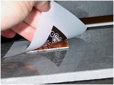
3. Secure the paper and board firmly in place, ensuring no movement occurs.
4. Utilize heat, using either an iron box or alternative heat sources, on the white printed paper.
5. Carbon powder is sprayed onto the white paper at the printing machine. By applying heat, the model is scanned, causing the carbon powder to adhere to the paper. Any excess powder remaining on the paper is then removed.
6. Following a similar procedure, position the printed paper’s surface onto the copper layer and apply heat. Consequently, the carbon powder adheres to the copper layer, effectively fusing the paper to the board.
7. Immerse the board in water and gently remove the paper. This process results in the carbon layer being affixed to the copper board. An illustrative image demonstrating this process is depicted in the figure below.
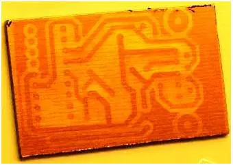
Next, immerse the board in ferric chloride solution. Subsequently, the copper undergoes a reaction with the ferric chloride, where the copper lacking a carbon layer dissolves in the solution. The portion containing the carbon layer remains unaffected by the ferric chloride and remains intact. An illustrative image exemplifying this process is depicted in the figure below.
9. Proceed by using sandpaper to cleanse the board. Eliminate the carbon layer by gently scraping the board’s surface with the sandpaper. This action results in the complete removal of the carbon layer, revealing the copper layer beneath.
10. Create the necessary holes by drilling in accordance with the designated drill position layer.
11. Subsequently, accurately position the appropriate components in their designated places and affix them to the board using a soldering kit.
12. Trim any excess pins protruding from the holes using a cutter as the final step. This completes the assembly of our circuit.
- What is Proteus used for?
Proteus is used for schematic capture, SPICE simulation, and PCB layout via ISIS and ARES. - How do you select components in Proteus?
Use Library > Pick Device/Symbol or the left toolbar component mode to add components to the devices list. - Can Proteus simulate the circuit before making a PCB?
Yes, Proteus allows virtual simulation and debugging of the circuit before PCB design. - How is the board perimeter created in ARES?
Use the 2D graphics box mode, select board edge in layer selection, then draw the box on Work Space to form the perimeter. - What tool helps automatically route tracks in Proteus?
The shape-based auto-router in ARES can auto-route tracks and typically produces dual-layer PCBs. - How should the bottom copper layer be printed for etching?
Print only bottom copper and board edge, set scale to 100%, rotation horizontal, and select mirror reflection. - What etchant is used to remove unwanted copper?
Ferric chloride solution is used to dissolve copper not protected by the transfer carbon layer. - How do you transfer the printed layout onto the copper board?
Place the mirror-printed paper on the copper, apply heat to transfer the carbon layer, soak to remove paper, leaving the carbon on copper. - What should be done after etching and cleaning the board?
Sand off the carbon, drill holes per drill plot layer, place and solder components, then trim excess leads.