
Summary of 45W USB-PD SMPS REFERENCE DESIGN DELIVERS 21.5W/IN3
The REF_XDPS21071_45W1 is a compact 45W USB-PD Type C charger reference design by Infineon. It utilizes the digital flyback controller XDPS21071 with CoolMOS and OptiMOS transistors to achieve 90% peak efficiency across universal input voltages (90-264 Vac). The design supports multiple output profiles (5V to 20V) while meeting strict regulatory limits through features like Zero Voltage Switching (ZVS), adaptive burst mode, and comprehensive protection circuits for high reliability in small form factors.
Parts used in the REF_XDPS21071_45W1:
- Infineon digital flyback controller XDPS21071
- 700V CoolMOS™ P7 Superjunction MOSFET IPD70R360P7S
- OptiMOS™ PD synchronous-rectification MOSFET BSC0805LS
- Small-signal-MOSFET BSL606SN
- ZVS winding
- ZVS circuit driven by GD1 pin
- HV start-up cell
- Resistor RHV (102kΩ)
The REF_XDPS21071_45W1 from Infineon is a 45W USB-PD type C charger reference design in a small form factor. The reference design has been developed to demonstrate the performance by meeting various regulatory limits as well as allowing for small form factor designs.
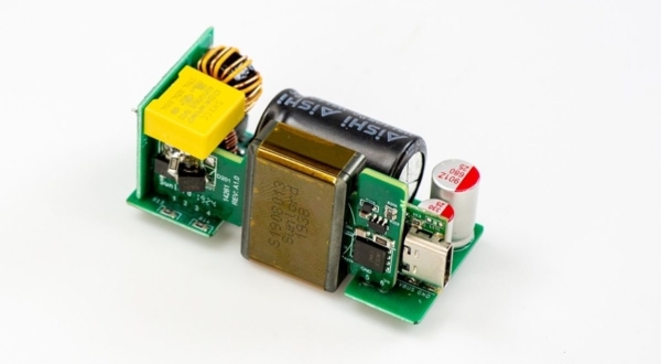
It features Infineon’s digital flyback controller XDPS21071, 700V CoolMOS™ P7 Superjunction MOSFET (IPD70R360P7S), OptiMOS™ PD synchronous-rectification MOSFET (BSC0805LS) and small-signal-MOSFET (BSL606SN).
This 45W USB-PD 3.0 type C charger has a universal input voltage range of 90- to 264-Vac. The supported output is 5V/3A, 9V/3A, 12V/3A, 15V/3A and 20V/2.25A. Its peak efficiency is 90%, with a low standby input power of <30mW.
Circuit Overview
The REF_XDPS21071_45W1 circuit is similar to a typical flyback converter design with SR in the secondary high-side. The XDPS21071 is a cycle-by-cycle peak current flyback controller with secondary-side control by means of a MFIO pin. The particular design can achieve close to ZVS with the help of an additional ZVS winding and ZVS circuit driven by the GD1 pin.
With the ZVS feature, the switching loss is reduced significantly at high-line so that the switching frequency can be set at around 140kHz. For low-line, the system would run in DCM operation. Besides having high efficiency at full load, the controller can achieve high efficiency at both medium and light load by implementing FRM and ABM. The controller integrates a HV start-up cell. Connected with a resistor, RHV (102kΩ) from the bulk capacitor, it can achieve VCC start-up charging and also the brown-in and brown-out features.
In addition, it has various protection features to protect the system from hazards, such as OCP, Vout OVP, OLP, OTP, latch enable, CS pin short before power-up, etc.
Read more: 45W USB-PD SMPS REFERENCE DESIGN DELIVERS 21.5W/IN3
- What is the peak efficiency of this charger?
The peak efficiency is 90%. - Can this design operate with universal input voltage?
Yes, it supports a universal input voltage range of 90- to 264-Vac. - How does the design reduce switching loss at high-line?
It uses a ZVS feature with an additional ZVS winding and circuit to significantly reduce switching loss. - Does the controller support light load efficiency?
Yes, it achieves high efficiency at medium and light loads by implementing FRM and ABM. - What are the supported output voltage levels?
It supports 5V/3A, 9V/3A, 12V/3A, 15V/3A, and 20V/2.25A. - Is there a startup mechanism for VCC charging?
Yes, an integrated HV start-up cell connected with a 102kΩ resistor achieves VCC start-up charging. - Does the system include protection against over-temperature?
Yes, it includes OTP (Over Temperature Protection) among other hazard protections.
