Summary of How to drive 595 shift registers with AVR hardware SPI
This article explains how to drive shift registers using an AVR chip's built-in SPI hardware. It details connecting control pins like SCLR and Enable, linking SI, SCK, and RCK, and cascading multiple chips. The process involves configuring the microcontroller for SPI Master mode, pulling the SS pin low, writing data to the SPDR register, and toggling the latch to update outputs.
Parts used in the Shift Register Project:
- AVR chip (ATmega168)
- Shift register chips
- SPI module
- Clear pin (SCLR)
- Enable pin
- Serial In pin (SI)
- Serial Clock pin (SCK)
- Storage Clock pin (RCK)
- Latch mechanism
- LEDs
Driving a shift register using an AVR chip’s built-in hardware is really quite easy. Most of their offerings have an SPI module, or Serial Peripheral Interface. A shift register is exactly that, a peripheral device that communicates via a serial line. All we need to do is hook up our connections and use a few pieces of simple code. Join me after the break to see how that’s done.
Just want to know how shift registers work? Check in on my other post on that topic.
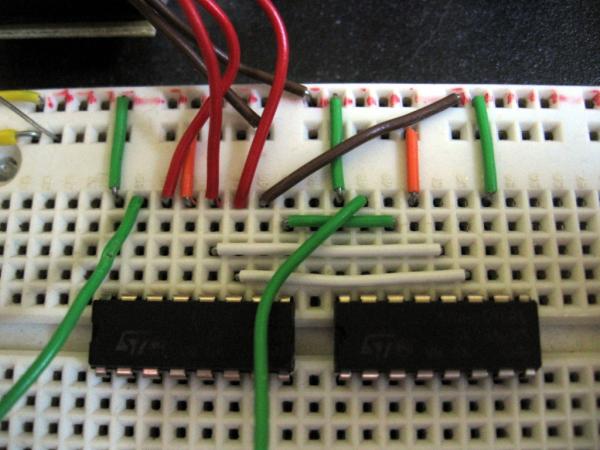
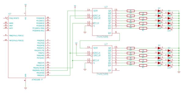
The first thing to consider is that it may not be necessary to connect the Clear and Enable pins to the microcontroller. If there are relatively few shift registers being used together it may be easier to shift in all zeros and latch them to the registers. But if timing is a big issue you may want this capability. For this example I have just connected the SCLR pin to VCC and the enable pin to GND.
This leaves three control pins: SI, SCK, and RCK. It is possible to drive SCK and RCK from the same signal, but that’s for another tutorial. My test hardware, the ATmega168, has pins meant to drive each of these controls. Note that the serial and storage clocks (SCK and RCK) for both shift register chips are hooked together on two data buses. The Serial In of the first chip (SI) is connected to the microcontroller. The QH prime pin of this first chip is connected to the SI pin of the second chip to cascade the data from one to the next.
Using the AVR SPI hardware
Accessing the SPI hardware is pretty simple. There’s only a few things that need to happen to get it running:
- Define which pins we’re using and set them to outputs
- Enable SPI and set it to Master mode
- pull the SS pin low
- Write our data to the SPDR, it will automatically be strobed into the shift registers
- Toggle the latch to display the data on the LEDs
The definitions are easy enough. I can’t just choose any pins, the SPI outputs are specific pins which can be looked up in the datasheet:
Read More: How to drive 595 shift registers with AVR hardware SPI
- How do I connect the Clear and Enable pins?
You can connect the SCLR pin to VCC and the enable pin to GND for this example. - What are the three main control pins required?
The three control pins are SI, SCK, and RCK. - Can SCK and RCK be driven by the same signal?
Yes, it is possible to drive both from the same signal, though this is covered in another tutorial. - How do I cascade data between two shift register chips?
Connect the QH prime pin of the first chip to the SI pin of the second chip. - What steps are needed to access the SPI hardware?
Define pins as outputs, enable SPI in Master mode, pull the SS pin low, write data to SPDR, and toggle the latch. - Where can I find the specific pins for SPI outputs?
The specific pins for SPI outputs are listed in the microcontroller datasheet. - Does the serial clock need to be different for each chip?
No, the serial and storage clocks for both shift register chips are hooked together on two data buses. - What happens when data is written to the SPDR register?
The data will automatically be strobed into the shift registers.