
Summary of TWO BITS PER TRANSISTOR: HIGH-DENSITY ROM IN INTEL’S 8087 FLOATING POINT CHIP
The 8087 chip, introduced by Intel in 1980, significantly accelerated floating-point arithmetic for early IBM PCs by utilizing a unique multi-level ROM storing two bits per transistor. This high-density design allowed the chip to fit necessary microcode within its 40,000-transistor limit. The article details the reverse engineering of the die, highlighting functional blocks like fraction processing and exponent circuitry that enabled operations up to 100 times faster than integer-only processors.
Parts used in the Intel 8087 Floating Point Chip:
- Multi-level ROM (Read-Only Memory)
- Transistors
- Microcode storage
- Fraction processing circuitry
- Storage of constants
- 64-bit shifter
- 64-bit adder/subtracter
- Register stack
- Exponent processing circuitry
The 8087 chip provided fast floating point arithmetic for the original IBM PC and became part of the x86 architecture used today. One unusual feature of the 8087 is it contained a multi-level ROM (Read-Only Memory) that stored two bits per transistor, twice as dense as a normal ROM. Instead of storing binary data, each cell in the 8087’s ROM stored one of four different values, which were then decoded into two bits. Because the 8087 required a large ROM for microcode1 and the chip was pushing the limits of how many transistors could fit on a chip, Intel used this special technique to make the ROM fit. In this article, I explain how Intel implemented this multi-level ROM.
Intel introduced the 8087 chip in 1980 to improve floating-point performance on the 8086 and 8088 processors. Since early microprocessors operated only on integers, arithmetic with floating point numbers was slow and transcendental operations such as trig or logarithms were even worse. Adding the 8087 co-processor chip to a system made floating point operations up to 100 times faster. The 8087’s architecture became part of later Intel processors, and the 8087’s instructions (although now obsolete) are still a part of today’s x86 desktop computers.
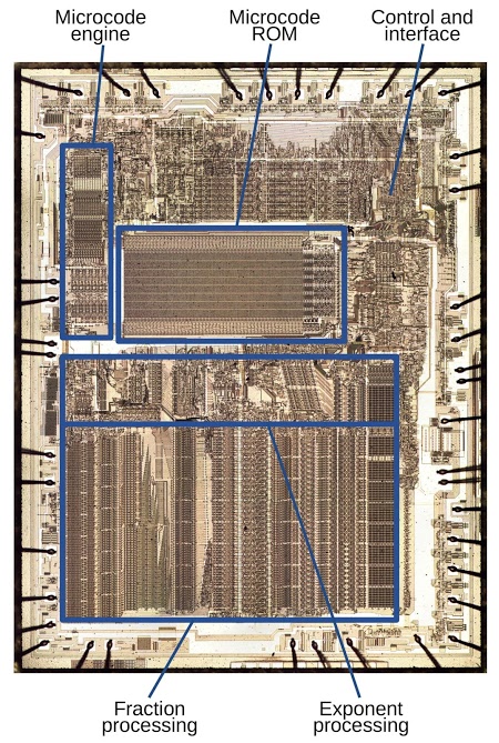
I opened up an 8087 chip and took die photos with a microscope yielding the composite photo below. The labels show the main functional blocks, based on my reverse engineering. (Click here for a larger image.) The die of the 8087 is complex, with 40,000 transistors.2 Internally, the 8087 uses 80-bit floating point numbers with a 64-bit fraction (also called significand or mantissa), a 15-bit exponent and a sign bit. (For a base-10 analogy, in the number 6.02×10²³, 6.02 is the fraction and 23 is the exponent.) At the bottom of the die, “fraction processing” indicates the circuitry for the fraction: from left to right, this includes storage of constants, a 64-bit shifter, the 64-bit adder/subtracter, and the register stack. Above this is the circuitry to process the exponent.
Read more: TWO BITS PER TRANSISTOR: HIGH-DENSITY ROM IN INTEL’S 8087 FLOATING POINT CHIP
- What was the primary purpose of the 8087 chip?
The 8087 was introduced to improve floating-point performance on the 8086 and 8088 processors. - How much faster were floating point operations with the 8087?
Adding the 8087 co-processor made floating point operations up to 100 times faster. - Why did Intel use a multi-level ROM in the 8087?
Intel used this technique because the chip required a large ROM for microcode and was pushing the limits of transistor density. - How many bits does each cell in the 8087's ROM store?
Each cell stored one of four different values which were decoded into two bits. - What is the internal structure of the numbers processed by the 8087?
The 8087 uses 80-bit floating point numbers consisting of a 64-bit fraction, a 15-bit exponent, and a sign bit. - How many transistors are inside the 8087 die?
The die of the 8087 contains 40,000 transistors. - Which components are included in the fraction processing block?
The fraction processing block includes storage of constants, a 64-bit shifter, the 64-bit adder/subtracter, and the register stack. - Are the instructions from the 8087 still used today?
Yes, although now obsolete, the 8087's instructions are still part of today's x86 desktop computers.