A related article on this site: True RMS-To-DC Adaptor for DVM
Introduction
This project came about when I needed to perform some reliability tests on some headphones according to IEC 268-7. The test requires operating the headphones at their rated input power for a number of hours using clipped pink noise, and muting the noise periodically during the test. There are plenty of white noise generators around, but this test called for a specific filter and that the signal be clipped such that the ratio of peak voltage to RMS voltage is between 1.8:1 2.2:1. More conventionally, we would say that the crest factor is set to 2.0 ±10%. Not having a budget for that specialized equipment but having a large stock of components, I opted to make the noise generator myself.
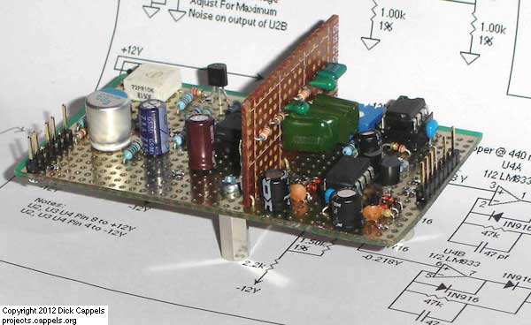
The noise generator shown in Photo 1 requires a regulated power supply of +12 and -12 volts. It provides 438 mv P-P clipped pink noise on one output, and white noise and un-clipped pink noise on two other outputs. All of the outputs are connected directly to the outputs of op amps and are not intended to drive long cables or other capacitive loads.
The specification for the clipped pink noise signal can be found in International Standard IEC 268-7 Sound Equipment, Part 7: Headphones and earphones; Section 3.3.2.2, Method of Measurement. The pink filter and its response are shown in International Standard IEC 268-7 Sound Equipment, Part 1: General; Figures 1 and 2.
The circuit, shown in Figure 1, is composed of a Zener diode white noise source and its bias supply and a preamplifier. This gets the noise up to the 10 to 20 mv RMS level. A second gain stage provides another 31 db of gain, making the noise signal amplitude sufficient to drive the Pink filter described in EN 268-1. The filter is followed by another 31 db fixed gain amplifier than an amplifier with adjustable gain, followed by the clipper circuit. The adjustable gain stage is to allow adjustment of ratio of Peak to RMS noise.
A transistor switch in the clipper circuit allows muting by shunting the noise signal to ground when biased on.
Several methods of generating noise are discussed on the internet (such as this article on this very website). After some careful consideration, I decided that a Zener diode based noise source would provide pretty clean and stable “white” noise. What convinced me was a paper written P.I. Somlo in 1975 in which the suitability of a 6.2 volt Zener diode as a transfer noise standard was discussed.
In his paper, Somlo noted that Zener diodes with a nearly zero temperature coefficient of voltage were also the most stable in terms of noise output as a function of temperature. The Somlo paper can be read at users.cosylab.com/~msekoranja/tmp/04236738.pdf Somlo mentioned a distinct “hump” in the function of noise vs current.
The method of biasing the Zener diode was influenced by Linear Technology Design Note 70 in which Jim Williams described a white noise generator.
As shown in Figure 2, the TL431 bias supply sets the voltage across the 25.5k metal film resistor. It was noted by Somlo and others that noise as a function of current has a peak followed by a valley, followed by another peak, indicating two distinct modes of operation. The first peak can be seen in Figure 3 below, in which RMS noise is plotted against voltage from the bias voltage source into the 25.5k resistor.

