
Summary of Analog Devices’ High-Speed Multi-Channel Analog-to-Digital Converters Reduce System Board Space : – ADI’s AD9239 and AD9639 quad 12-bit analog-to-digital converters use 50 percent less PCB area, yielding space savings for high-bandwidth data acquisition applications.
The article introduces the AD9239 and AD9639, high-speed quad ADCs from Analog Devices. These devices feature on-chip PLLs, input buffers, and temperature sensors for thermal monitoring. They operate with a single 1.8-V supply, offering low power consumption and excellent noise performance, including an SNR of 65 dBFs and ENOB of 10.5 bits at 85 MHz. The AD9239 uses packetized output, while the AD9639 supports JESD204-compliant output. Both provide LVDS-compatible clock inputs and coded serial data streams.
Parts used in the AD9239 and AD9639 Project:
- AD9239 ADC
- AD9639 ADC
- On-chip PLL (phase-locked loop)
- Input buffer circuits
- On-chip temperature sensor
- LVDS-compatible sample-rate clock input
- Four serial digital output streams
- VisualAnalog evaluation tool
- ADIsimADC behavioral software modeling tools
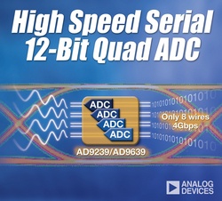
NORWOOD, Mass. (PRWEB) November 19, 2008
The 250-MSPS (mega-sample-per-second) AD9239 incorporates an efficient packetized output scheme, while the 210-MSPS AD9639 supports a JESD204-compliant output scheme. Both ADCs feature on-chip PLL (phase-locked loop) and input buffer circuits, which are designed for low cost, low power, small size, and ease of use. The new ADCs require a single 1.8-V power supply, dissipating 1.5 W in normal mode and 145 mW per channel (typical) when standby-mode is enabled with the digital link remaining in operation. The new devices are also the first high-speed ADCs to feature an on-chip temperature sensor, which allows engineers to conduct thermal monitoring for optimized system operation. The quad ADCs offer excellent noise performance and achieve SNR (signal-to-noise ratio) of 65 dBFs, SFDR (spurious-free dynamic range) of 77 dBc and an ENOB (effective number of bits) of 10.5, all at an 85-MHz input frequency.
The AD9239 and AD9639 support an LVDS (low-voltage differential signal)-compatible sample-rate clock input and provide four serial digital output streams with coded data from each ADC channel. Clock information is also coded into each serial stream so that the receiving logic can extract the necessary clocking information. The AD9239 and AD9639 are available with ADI’s VisualAnalog evaluation and ADIsimADC behavioral software modeling tools.
Availability and Pricing
Product
- What is the maximum sampling rate of the AD9239?
The AD9239 operates at 250-MSPS. - Can these ADCs be powered by a single voltage source?
Yes, they require a single 1.8-V power supply. - Does the device include a method for thermal monitoring?
Yes, they are the first high-speed ADCs to feature an on-chip temperature sensor. - What is the typical power dissipation per channel in standby mode?
The typical power dissipation is 145 mW per channel when standby-mode is enabled. - How many serial digital output streams do these ADCs provide?
They provide four serial digital output streams with coded data from each ADC channel. - Does the output stream contain clock information?
Yes, clock information is coded into each serial stream so receiving logic can extract it. - What software tools support the AD9239 and AD9639?
They are available with ADI's VisualAnalog evaluation and ADIsimADC behavioral software modeling tools. - What is the SNR achieved at an 85-MHz input frequency?
The devices achieve an SNR of 65 dBFs at an 85-MHz input frequency.
