Summary of ATMega32 Microcontroller: The Ultimate Guide for Beginners
The ATMega32 is an 8-bit Atmel microcontroller offering more I/O pins than the ATMega328P, with dedicated pins for digital I/O, analog ADC channels, PWM, timers, serial interfaces (UART, SPI, I2C), external interrupts, JTAG, comparator, and power/oscillator functions. Its RISC CMOS design balances performance and power, enabling simultaneous use of multiple peripherals via dedicated pin assignments and accessible port registers for flexible embedded applications.
Parts used in the ATMega32 Project:
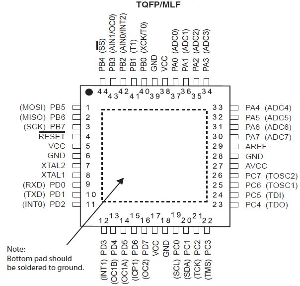
- ATMega32 microcontroller (TQFP/MLF package)
- Power supply (VCC)
- Ground connections (GND)
- Analog reference capacitor or connection (AREF)
- Analog power input (AVCC)
- Crystal oscillator or external clock (XTAL1, XTAL2)
- Port A headers for ADC inputs (PA0–PA7 / ADC0–ADC7)
- Port B headers for digital I/O and SPI pins (PB0–PB7; SS, MOSI, MISO, SCK)
- Port C headers for digital I/O, I2C, and JTAG (PC0–PC7; SCL, SDA; TDI, TDO, TMS, TCK)
- Port D headers for digital I/O, UART, interrupts, timers, and PWM (PD0–PD7; RXD, TXD; INT0, INT1, INT2; T0, T1; OC pins)
- External oscillator pins/connectors for Timer oscillators (TOSC1, TOSC2)
The ATMega32 is an widely used microcontroller from Atmel. It shares many similarities with the ATMega328P but has a more reduced memory capacity. However, the ATMega32 makes up for this with a greater number of input/output pins available.
A key advantage of the ATMega32 is that each GPIO pin can exclusively support either digital input/output or analog functions. This allows developers to utilize all of the microcontroller’s various communication protocols simultaneously. Peripherals can interact and pass data directly within the chip via dedicated pin assignments.
Built on an 8-bit CMOS technology using Atmel’s RISC architecture, the ATMega32 is optimized to efficiently balance performance and power consumption via software programming. The simplified pin architecture streamlines development while its integrated peripheral features continue to make the ATMega32 a versatile and cost-effective microcontroller suitable for a wide range of embedded applications.
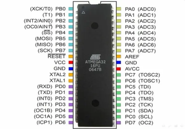
Pinout Diagram ATMega32
The ATMega32 utilizes its full pin complement, providing developers with ample input/output accessibility. Crucially, each pin is dedicated to support a specific communication protocol or peripheral function. This allows the microcontroller’s capabilities to be maximally exploited through software programming.
An overview of the pin assignments and their associated functions:
Digital I/O pins: Can be configured for use as general purpose I/O for interfacing with external devices.
Analog input pins: Support analog to digital conversion for reading analog sensor values.
PWM output pins: Provide pulse width modulation signal generation for applications like motor control.
Serial communication pins: Dedicated toynchronous (USART) and I2C (TWI) serial interfaces enable data transfer with peripherals and other microcontrollers.
Timer/Counter pins: Used with on-chip timer/counters for tasks like pulse measurement and generation.
External interrupt pins: Can sense external state changes to trigger interrupt service routines.
By leveraging dedicated pin assignments, developers benefit from direct peripheral access without need for multiplexing. This maximizes the ATMega32’s potential as a flexible embedded microcontroller.
This diagram is an ATMega32 Pin layout of TQFP and MLF Package.
Pin Configuration Details
Digital Input/Output
Input and output pins are essential for a microcontroller to interface with external devices and the environment. The ATMega32 provides a generous allotment of 32 I/O pins to support these interactions.
As an CMOS integrated circuit, any pin can be utilized as a digital input/output. Pin voltages will not exceed the applied power supply level, and inputs should also not surpass the power level.
The pins are directly associated with the microcontroller’s port registers – Port A, B, C and D. This allows for low-level control of pin attributes like direction and state. Each pin incorporates an internal pull-up resistor as well, for flexible logic level functionality.
An overview of the ATMega32’s available I/O pins is:
(List of pin numbers and their associated ports)
This comprehensive assortment of general purpose digital pins grants developers ample flexibility in designing circuits. Combined with individually accessible port registers, it supports interfacing with a wide range of external digital devices and sensors.
- PA0 – GPIO40
- PA1 – GPIO39
- PA2 – GPIO38
- PA3 – GPIO37
- PA4 – GPIO36
- PA5 – GPIO35
- PA6 – GPIO34
- PA7 – GPIO33
- PB0 – GPIO0
- PB1 – GPIO1
- PB2 – GPIO2
- PB3 – GPIO3
- PB4 – GPIO4
- PB5 – GPIO5
- PB6 – GPIO6
- PB7 – GPIO7
- PC0 – GPIO22
- PC1 – GPIO23
- PC2 – GPIO24
- PC3 – GPIO25
- PC4 – GPIO26
- PC5 – GPIO27
- PC6 – GPIO28
- PC7 – GPIO29
- PD0 – GPIO14
- PD1 – GPIO15
- PD2 – GPIO16
- PD3 – GPIO17
- PD4 – GPIO18
- PD5 – GPIO19
- PD6 – GPIO20
- PD7 – GPIO21
Interrupt Pins
Interrupt pins play an important role for microcontrollers to react to external stimuli in a timely manner. As circuit complexity increases due to physical constraints, more interrupt pins are often necessary.
The core function of interrupt pins is to request the CPU’s attention when a connected device requires a service. The microcontroller’s programmed interrupt service routine will suspend current code execution and instead perform dedicated instructions in response to the external pulse on the interrupt pin.
The ATMega32 provides three such pins for interrupt handling. A benefit is that all three can be used simultaneously without interference. This allows independent prioritization of interrupts from multiple sources.
The three interrupt pins available on the ATMega32 are:
(List of pin numbers and associated interrupt vectors)
By supporting interrupts on dedicated pins, the microcontroller can effectively serve external devices in a non-blocking manner. This facilitates responsive functionality for a variety of real-time embedded applications.
- INT0 – GPIO16
- INT1 – GPIO17
- INT2 – GPIO3
ATMega32 Serial Communication Ports:
Asynchronous Serial
The ATMega32 provides support for several serial communication protocols. One of the most commonly used is asynchronous serial, or UART, communication.
UART communication is popular due to its simplicity and easy implementation through programming. It relies on just two pins – one for transmitting data and another for receiving data.
The ATMega32 has a dedicated module that handles asynchronous serial functionality. Key aspects of this UART module include:
(Describe UART module, its main features like independent RX/TX buffers, baud rate control registers, interrupt handling etc.)
By incorporating a full-featured UART module, the microcontroller seamlessly integrates asynchronous serial functionality. This makes it well-equipped to interface with a wide variety of peripherals that employ standard UART protocols for data transfer and control. Programmers can leverage the UART for robust serial communication in their embedded designs.
- RXD – GPIO14
- TXD – GPIO15
Synchronous Serial
While asynchronous and synchronous serial communication share many similarities, there is an important difference in the clock source. In asynchronous serial protocols, each device derives its own clock internally via software programming.
However, synchronous serial communication requires an externally supplied clock signal to precisely synchronize data transfers between connected devices. This external clock signal is transmitted through dedicated input/output pins.
The ATMega32 microcontroller incorporates such a pin to support synchronous serial functionality. When utilizing synchronous serial protocols, an external clock signal can be received on this pin to keep transmitted and received data frames matched in timing.
This clock I/O pin allows the ATMega32 to interface with peripherals that expect accurate clocking information via wired serial standards like SPI and I2C. It helps overcome the limitations of asynchronous communication for applications where tight synchronization is essential.
- XCK – GPIO1
SPI
SPI (Serial Peripheral Interface) is another commonly used serial communication standard due to its capacity to handle multiple devices simultaneously.
It utilizes four pins for connectivity – two for bidirectional data transfer, one for clock signal generation, and an optional fourth pin. When a single device is connected, the fourth pin is unused.
However, in applications requiring connection to multiple SPI slaves, the fourth pin takes on an important role as a Select Slave (SS) pin. Only the selected slave will respond during data transfers while others remain deselected.
The ATMega32 contains dedicated SPI hardware supporting communication using just four pins – MOSI, MISO, SCK and an optional SS pin. While it can directly interface with a single SPI device using those pins, multiple devices can also be managed through software by defining additional SS pins on other I/O lines.
This provides flexibility to leverage the ATMega32’s SPI module for both single and multiple-device configurations through judicious use of its pin resources and programming techniques.
- SS’ – GPIO5
- MOSI – GPIO6
- MISO – GPIO7
- SCK – GPIO8
I2C
I2C (Inter-Integrated Circuit) is another serial communication standard, but it is well-suited for applications needing predominantly one-way data transfer. For this reason, it is commonly found in sensors, LCD displays, motors and other peripherals that transmit readings or receive control signals.
I2C relies on just two bi-directional pins – one for data line communications and the other dedicated to the clock. By multiplexing these two lines, up to 128 devices can be addressed on the same bus.
The ATMega32 contains the following pins to support its on-board I2C functionality:
SDA pin (I2C Data)
SCL pin (I2C Clock)
By implementing the I2C protocol in hardware, the microcontroller can easily interface with a wide range of compact peripherals. These commonly transmit analog sensor readings or require simple commands over the I2C bus, exploiting its low bandwidth needs.
- SCL – GPIO22
- SDA – GPIO23
Analog to Digital Channel
The ATMega32 features an onboard 10-bit Analog-to-Digital Converter (ADC) module capable of servicing 8 independent analog input channels.
All 8 channels are multiplexed through a single ADC hardware unit, allowing it to convert multiple channel values simultaneously. The analog inputs are accessed via Port A pins alone.
The 8 ADC channels available on the ATMega32 are:
(List port A pin numbers for each ADC channel)
By concentrating all analog pin options on a single port, the ADC’s 10-bit resolution can be leveraged across the different channels in parallel. This efficient design is well-suited for applications involving multiple sensors or signals that must be sampled contemporaneously.
Programmers can take advantage of the ATMega32’s on-chip ADC and its ability to concurrently digitize readings from all sensor channels connected to Port A.
- ADC0 – GPIO40
- ADC1 – GPIO39
- ADC2 – GPIO38
- ADC3 – GPIO37
- ADC4 – GPIO36
- ADC5 – GPIO35
- ADC6 – GPIO34
- ADC7 – GPIO33
Timer Module Pins
The ATMega32 provides three separate timer modules to enable precise timing and pulse generation capabilities.
Timer 0 and Timer 1 are both 8-bit timers that can count external events input through dedicated pins. In contrast, Timer 2 is a larger 16-bit timer intended for internal event counting.
All timers can be clocked by the microcontroller’s primary oscillator or an optional secondary oscillator connected via specific pins. This secondary oscillator affords tailored frequency control over the timers as needed.
The timer modules and associated clock pins on the ATMega32 include:
Timer 0 (8-bit): Can be driven by external oscillator on pin.
Timer 1 (8-bit): Can be driven by external oscillator on pin.
Timer 2 (16-bit): For internal timing without external pin.
OSC0 pin: Secondary oscillator input for Timer 0.
OSC1 pin: Secondary oscillator input for Timer 1.
This set of versatile timer resources supports timing applications requiring precision from microseconds to days.
- T0 – GPIO1
- T1 – GPIO2
- TOSC1 – GPIO28
- TOSC2 – GPIO29
Capture/Compare/PWM
The ATMega32 provides certain pins that can generate configurable output waveforms through pulse-width modulation (PWM) techniques.
When configured as PWM pins, they will monitor input signals and compare them against programmed values. On each match, the pin will generate a pulse or toggle its state.
Developers can leverage these pins to produce precision PWM outputs for functions like motor speed control, LED dimming, or digital-to-analog conversion.
The ATMega32 pins capable of pulse-width modulated outputs are:
(List port and pin numbers of PWM pins)
By utilizing the microcontroller’s onboard PWM functionality, designers gain precise timing outputs without additional components. This empowers projects involving servo motors, Neopixel LEDs, and more through direct pin actuation instead of external PWM controllers.
- OC0 – GPIO4
- OC1B – GPIO18
- OC1A – GPIO19
- OC2 – GPIO21
ICP
While some pins on the ATMega32 can generate PWM outputs, there is also a dedicated input referred to as the Input Capture (ICP) pin.
This pin serves to sample external PWM signals coming into the microcontroller. By monitoring the ICP pin, developers can determine timing characteristics like the frequency and duty cycle of an incoming PWM waveform.
The primary function of the ICP pin is to capture the external PWM input for analysis. Parameters extracted from the sampled PWM signal can then be used for purposes such as RPM measurement, servo position decoding, or feedback control algorithms.
Compared to PWM output pins focused on signal generation, the ICP pin provides the inverse capability – sampling an external PWM source for further digital processing instead of analog output actuation. This expands the microcontroller’s monitoring role beyond signal generation.
- ICP1 – GPIO20
ICP1 uses timer1 which is an 8-bit timer.
Comparator Pins
The ATMega32 features an internal comparator designed for comparing analog input signals, with two pins at your disposal. One of these pins, labeled as GPIO3, is utilized for non-inverted signals, while the other, labeled as GPIO4, is designated for inverted signals. The analog compared signal can be harnessed by internal registers for various applications.
- AN0 (non-inverted) – GPIO3
- AN1 (inverted) – GPIO4
JTAG Programmer Pins
The company introduced JTAG pins for debugging and testing microcontrollers. The ATMega32 microcontroller is equipped with JTAG communication pins, which can also serve for programming the microcontroller. The following are the JTAG pins:
- TDI – GPIO27
- TDO – GPIO26
- TMS – GPIO25
- TCK – GPIO24
Power Pins of ATMega32
AREF
The ATMega32’s ADC relies on the microcontroller’s power source to assess varying analog input signal levels. Occasionally, this feature produces unanticipated readings. The highest analog signal value is indicated through voltage on the reference pin.
- AREF – Pin32
AVCC
The microcontroller’s Analog to Digital converter necessitates an external voltage input for activation and proper operation. The analog power pin for the ATMega32 is:
- AVCC – GPIO30
Power Input
All devices necessitate a power source for their functionality. The ATMega32 includes three power pins, one designated for power input, and the remaining two serving as ground connections. These power pins encompass:
- VCC – GPIO10
- GND – GPIO11, GPIO31
Oscillator
The ATMega32 comes equipped with an internal clock running at 8MHz, and this clock frequency can be increased to 16MHz by connecting external clock pins.
- XTAL2 – GPIO12
- XTAL1 – GPIO13
Source: ATMega32 Microcontroller: The Ultimate Guide for Beginners
- What architecture does the ATMega32 use?
The ATMega32 is built on an 8-bit CMOS using Atmel's RISC architecture. - How many general purpose I/O pins does the ATMega32 provide?
The ATMega32 provides 32 general purpose I/O pins across Ports A, B, C, and D. - Can ATMega32 pins be used simultaneously for different peripherals?
Yes. Each GPIO pin can exclusively support either digital I/O or analog functions, allowing multiple peripherals to be used simultaneously via dedicated pins. - What serial communication protocols does the ATMega32 support?
The ATMega32 supports asynchronous serial (UART), synchronous serial, SPI, and I2C (TWI). - Which pins are used for ADC inputs on the ATMega32?
The ADC channels use Port A pins: ADC0–ADC7 correspond to PA0–PA7 (GPIO40–GPIO33). - Which pins serve UART receive and transmit functions?
RXD is GPIO14 and TXD is GPIO15 for the UART. - What pins are used for SPI communication?
SPI uses SS (GPIO5), MOSI (GPIO6), MISO (GPIO7), and SCK (GPIO8). - Which pins are assigned to I2C on the ATMega32?
I2C uses SCL (GPIO22) and SDA (GPIO23). - How many external interrupt pins does the ATMega32 have?
The ATMega32 provides three external interrupt pins: INT0 (GPIO16), INT1 (GPIO17), and INT2 (GPIO3). - What are the power and oscillator pins of the ATMega32?
Power pins include VCC (GPIO10), GND (GPIO11, GPIO31), AVCC (GPIO30), and AREF (Pin32); oscillator pins are XTAL1 (GPIO13) and XTAL2 (GPIO12).