Summary of ATmega644 JTAG Debugger
This project details the design and implementation of a low-cost debugger for the ATmega644 microcontroller using a second ATmega644 as the debugging host. The system utilizes the IEEE 1149.1 JTAG interface and the On-Chip Debugger (OCD) to enable breakpoints, register access, memory reads/writes, and single-stepping via HyperTerminal. By replacing expensive commercial tools like the JTAG ICE mkII, this solution provides essential debugging capabilities for embedded systems development at a fraction of the cost.
Parts used in the ATmega644 JTAG Debugger:
- STK500
- Custom PC board (old version without safety diode)
- MAX233CPP
- RS232 Connector for custom PC board
- ATmega644 microcontrollers (2 units)
- Two pin flat jumper
- One pin jumper
- DIP sockets (8 units)
Introduction
The purpose of this project was to design and implement a debugger for the ATmega644 that communicated through its JTAG interface and was capable of controlling program execution by setting breakpoints and accessing registers and memory.
We have three main objectives in this report:
- To enable a user to properly download our code onto an ATmega644, connect and configure a target, and begin debugging. See our User Guide.
- To serve as documentation on the On-Chip Debugger for the ATmega family of MCUs. See the OCD Documentation.
- To detail how we structured and designed the debugger from the very bottom level (serial bit input) to upper level commands (i.e. memory reads). See Design Schematics and Overview.
High Level Design
Rationale
During our time in ECE 4760, we encountered situations in which our code did not function as expected. We found debugging with print statements to HyperTerminal and flashing LEDs to be both insufficient and occasionally unsafe. Thus, it would be very helpful to have a debugger for the ATmega644 that we could use to set breakpoints and step through our program with access to memory and registers. Such devices are often very expensive. Even the JTAG ICE mkII, which Atmel labels a low-cost debugging tool, is sold for approximately $300. Our project attempted to build a debugger for an ATmega644 using a second microcontroller that communicated with the target board via the JTAG interface. We hoped to emulate the basic functionality of the JTAG ICE mkII, with features such as setting breakpoints, reading and writing data registers, I/O registers, and memory, and single stepping.
Design Schematic and Overview
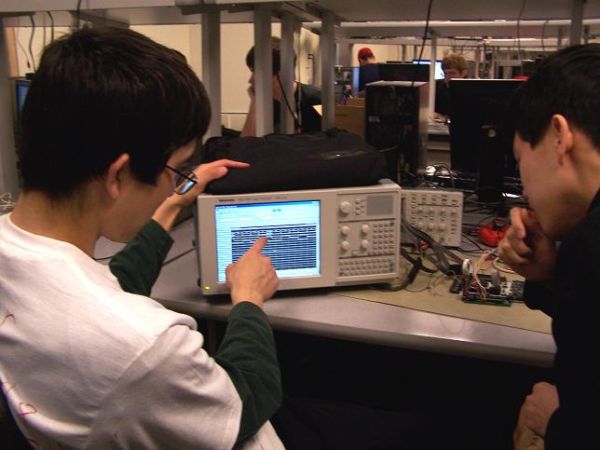
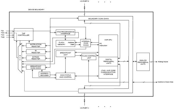
Our project consists of two ATmega644 MCUs. The microcontroller that we are debugging (referred to as the target) is programmed by the user with any arbitrary code. The other microcontroller (the debugger) contains the actual debugging firmware. The user is able to interface with the debugger through a command window on HyperTerminal. The debugging MCU is then able to control the target via the JTAG port. Our code running on the debugger sends a series of bits to the JTAG interface, which then stores it in the instruction / data registers of the JTAG. The JTAG interface is described in detail in the next section. The JTAG interface alone however does not allow us to perform all the necessary functions of our debugger. The ATmega644 contains an On-Chip Debugger unit, which is the module that can actually execute AVR instructions and set breakpoints.
We begin by describing the JTAG and OCD modules, including their respective registers, instruction sets, and communication protocols. Next, we discuss the design of our hardware and software, including an API describing each user function. Finally we discuss the results of our project.
Basic JTAG Overview
This project makes use of IEEE standard 1149.1, entitled Standard Test Access Port and Boundary-Scan Architecture. This standard was written by the Joint Test Action Group and is commonly referred to as JTAG. JTAG is commonly used to debug embedded systems and to program hardware devices. Companies like Atmel often provide JTAG interfaces on their products because of its popularity in industry. The ATmega644 comes with an On-Chip Debugger and an IEEE 1149.1 compliant JTAG interface.
The JTAG standard uses four signals: TCK, TMS, TDI, and TDO. TCK is a clock signal. TMS is the Test Mode Select signal which is used to navigate the JTAG state machine (See JTAG State Machine). TDI is the Test Data Input signal used to provide input for the JTAG interface. TDO is the Test Data Output signal used to retrieve the output data from the JTAG interface. These four signals are accessed through four port pins on the ATmega644 that are called the Test Access Port when using JTAG. Port pin C.2 is used for TCK, C.3 is used for TMS, C.4 is used for TDO, and C.5 is used for TDI. In order to use the Test Access Port, the JTAGEN fuse on the ATmega644 must be enabled. The IEEE standard also specifies a TRST signal, Test Reset, but this is an optional signal that is not used by the ATmega644.
JTAG State Machine
The JTAG standard is an implementation of the following state machine:
State transitions are controlled by the TMS signal, which is captured on the rising edge of TCK. The JTAG standard uses an Instruction Register, the contents of which determine the command to execute and which register to use as the Data Register. For example, if our IR content was 0x0, corresponding to the EXTEST instruction (See JTAG Instructions), then the multiplexer in the state machine would select the boundary scan chain register as the DR we would then shift data into. Likewise, if we wanted to access the OCD registers, we would first pass 0x08 into the instruction register. This would then select the Breakpoint Scan Chain as the DR.
To write to the Instruction Register, one must first navigate to the Shift-IR state. In this state, the TDI signal is captured on the rising edge of TCK and shifted into the Instruction Register. Data is shifted in one bit at a time, LSB first. TMS must remain 0 on the rising edge of TCK to stay in this state. When TMS is set to 1, it indicates that the MSB of the TDI data stream is being shifted in, and the Shift-IR state is exited. While shifting data into the Instruction Register, the data that was in the register, captured in the Capture-IR state, is shifted out to TDO, one bit at a time, on the falling edge of TCK. Reading from and writing to the selected Data Register can be accomplished the same way in the analogous DR states.
The Exit1, Pause, and Exit2 states are primarily used for state machine navigation. These can also be used to segment the data to shift in if there is not enough memory to shift one burst of data while in one of the Shift states.
The Update-IR state latches the instruction previously shifted into the Instruction Register on the falling edge of TCK. Once latched, the mode of operation is changed appropriately, including the selection of the appropriate Data Register. In the Update-DR state, the shifted in data is latched on the falling edge of TCK for registers with a latched parallel output.
The Run-Test/Idle state can be used as an idle state, and all of the methods we wrote returned the state machine to this state. There are certain testing instructions that can only be run in this state.
The Test-Logic-Reset state disables test logic and initializes the Instruction Register to contain the IDCODE instruction (See JTAG Instructions). Regardless of the current state, the Test-Logic-Reset state can be reached with five consecutive ones on TMS.
JTAG Instructions
To execute a JTAG instruction, a unique four bit code must be shifted into the Instruction Register. The following is a description of each instruction with its matching four bit code:
- IEEE 1149.1 Standard JTAG Instructions
-
- EXTEST 0x0: This instruction is used to perform a boundary scan. The Boundary-scan Chain is selected as the Data Register. On the ATmega644, performing a boundary scan returns the values of all port pins and their control bits.
- IDCODE 0x1: This instruction reports a version number, device number, and manufacturer code. The ID-Register is chosen as the Data Register.
- SAMPLE_PRELOAD 0x2: This instruction is used to pre-load the output latches and to take a snapshot of the I/O port pins without affecting system operations. This instruction is usually executed before executing the EXTEST instruction, since the EXTEST instruction will drive out the contents of the latched outputs of the Boundary-scan chain as soon as the EXTEST instruction is loaded.
- BYPASS 0xF: This instruction bypasses the boundary scan and simply sends the data shifted in from TDI directly out to TDO. The Bypass Register is chosen as the Data Register.
-
- AVR Specific JTAG Instruction:
- AVR_RESET 0xC: This instruction forces an AVR device into Reset mode. The single bit Reset Register is selected as the Data Register. If there is a 1 in the Reset Chain, the reset will remain active. When a 0 is shifted in, the AVR device will exit Reset mode and restart program execution.
On-Chip Debugger
The ATmega644 contains an On-Chip Debugger (OCD) that consists of a scan chain and a Breakpoint Unit, and it is capable of communication between the CPU and JTAG interface. The On-Chip Debugger was essential to the successful implementation of our debugger. The OCD contained the registers which configured and set the various breakpoints (described below). Also included was the On Chip Debugger Readback (OCDR) Register; this was the only IO Register belonging to the target board that the debugger could access through the JTAG port. Thus, with the OCDR, any register or memory location on the target board could be written to the OCDR, which the debugger could then read back.
It is important to note that the functions and registers of the OCD are all proprietary, and all original documentation is available only within Atmel. However, without knowledge of how to use the functions of the OCD, our project would have been impossible. We were able to find some documentation written by members of the Open Source community who had worked on creating a JTAG ICE mkII clone for the ATmega16. This documentation, although largely reliable, did have some inconsistencies with what we observed in our use of the OCD Registers. It is possible that this discrepancy could be due to differences between the ATmega16 and the ATmega644. We document below what we believe are the control and status bits of the On Chip Debugger registers for the ATmega644.
Description of OCD Registers
The OCD uses 16 16-bit registers. The On-Chip Debug Register (OCDR), OCD register 12, is used to provide communication between the CPU and JTAG interface. The other registers are listed below:
- 0 PSB0: This register is used to store a PC value to break on. The EN_PSB0 flag in the Break Control Register must be enabled to break on the stored value.
- 1 PSB1: This register is used to store a PC value to break on. The EN_PSB1 flag in the Break Control Register must be enabled to break on the stored value.
- 2 PDMSB: This register can either be used to break on a PC value or to break on data access. If PDMSB is storing a PC value to break on, then the EN_PDMSB, PDMSB0, and PDMSB1 flags in the Break Control Register must be set. If PDMSB is storing the address in memory to break on access, then the EN_PDMSB and PDMSB1 flags in the Break Control Register must be set.
- 3 PDSB: This register can either be used to break on a PC value or to break on data access. If PDSB is storing a PC value to break on, then the EN_PDSB, PDSB0, and PDSB1 flags in the Break Control Register must be set. If PDSB is storing the address in memory to break on access, then the EN_PDSB and PDSB1 flags in the Break Control Register must be set.
- 8 Break Control Register: This register contains flags to configure the OCD to break in the ways listed above. This includes breaking on a PC value, breaking on memory access, and breaking on change in program flow. The flags are ordered as follows:
Parts List:
| PART | COST |
|---|---|
| Total | $40 |
| 1 STK500 | $15 |
| 1 custom PC board (old version without safety diode) | $2 |
| 1 MAX233CPP | Free Sample |
| 1 RS232 Connector for custom PC board | $1 |
| 2 ATmega644s | $16 |
| 1 two pin flat jumper | $1 |
| 1 one pin jumper | $1 |
| 8 DIP sockets | $4 |
For more detail: ATmega644 JTAG Debugger
- What is the primary purpose of this project?
The purpose was to design and implement a debugger for the ATmega644 that communicates through its JTAG interface to control program execution by setting breakpoints and accessing registers and memory. - How does the debugger communicate with the target device?
The debugging MCU sends a series of bits to the JTAG interface, which stores them in the instruction or data registers of the JTAG to control the target. - Which signals are required for the JTAG standard used in this project?
The JTAG standard uses four signals: TCK (clock), TMS (Test Mode Select), TDI (Test Data Input), and TDO (Test Data Output). - Can the user set breakpoints using this debugger?
Yes, the On-Chip Debugger unit allows users to configure and set various breakpoints based on PC values or memory access. - What is the role of the OCDR Register in the ATmega644?
The OCDR Register is the only IO Register belonging to the target board that the debugger can access through the JTAG port to read back any register or memory location. - How much does the total hardware for this project cost?
The total cost for the parts listed in the project is $40. - Does the ATmega644 use the TRST signal for JTAG?
No, the TRST signal is an optional signal specified by the IEEE standard but is not used by the ATmega644. - What state must be reached to disable test logic and initialize the Instruction Register?
The Test-Logic-Reset state disables test logic and initializes the Instruction Register to contain the IDCODE instruction.