Summary of ATTiny Port Manipulation (Part 1): PinMode() and DigitalWrite()
This article explains how to replace Arduino's `pinMode()` and `digitalWrite()` functions with direct port register manipulation on ATTiny microcontrollers. This method offers significantly faster execution (roughly 40 times faster) and reduced memory usage by writing directly to hardware registers like DDRB and PORTB using bitwise operators. The guide details reading datasheets, understanding pin-to-port mappings, and implementing efficient code using operators like `|=`, `&=`, and `~`.
Parts used in the ATTiny Port Manipulation Project:
- ATTiny13A Microchip
- Arduino IDE
- LED
- Buzzer
- USB Connection
First off, this is written with Arduino and the Arduino IDE in mind. I will be referencing various Arduino sources and datasheets for AVR chips.
Secondly, what does this really mean?
Manipulation of port registers allow for lower-level and faster manipulation of the i/o pins of Arduino and on any ATTiny microchip.
Why would you want to do this?
The Arduino IDE and its coding is extremely user friendly. That is, it makes programming easier with the use of functions to accomplish tasks. In this case, pinMode() and digitalWrite(). These write commands to a certain pin. What you do not see is how the functions do this.
The short version is that they go through their own lines of code to do what you want it to. And this takes time. And in Micro controller time, it can be pretty significant if you are working on a particularly time sensitive project. Direct port manipulation is roughly 40 times faster at writing a command to a pin than the digitalWrite() function. Additionally, port manipulation saves on memory in the chip as it ends up being fewer lines of code being programmed into the controller/chip. Although, if this is your main reason for learning port manipulation, many would simply say that you are using the wrong chip.
If this is so beneficial, why doesn’t everyone do this?
Most will eventually wander into this area in their tinkering careers. But the biggest problem is, that this can be very intimidating and confusing to anyone new without someone sitting next to them explaining it. It gets into binary mathematics (not that you really need to understand that part), new commands you will not have seen up to this point, and it forces you to really learn to read understand a datasheet for a new microchip.
Step 1: Getting Familiar With a Datasheet
The following is a link to the datasheet for the ATTiny13A. This is a chip I am familiar with.
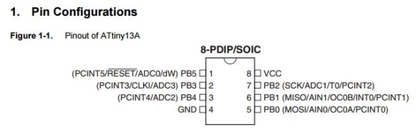
The first thing to know is the difference between Pins and Ports. A Pin is the physical metal part coming from the chip and the number ascribed to it given its location that chip.
A Port refers to a Pin given its function within a register.
This brings us to the term you have to learn, register. A register is a location in a store of data, used for a specific purpose and with quick access time. In this case, it’s a binary series that you can write 1s or 0s to in order to assign different functionalities to a port.
If you look at the first figure on page 2 of the link above, you will see the typical ATTiny13A version that would be used by the average tinkerer. You can see that it has 8 pins, most of which have multiple labels attached to them.
For example, Pin 3 is labelled as PCINT3, CLKI, ADC3, and PB3. This means that Pin 3 can be used as Pin Change Interrupt 3 (PCINT3), Clock In (CLKI), Analog to Digital Converter 3 (ADC3), and PORT B 3 (PB3). Pin 2 is always Pin 2 but also Port 3 in the PB register, for example.
Step 2:

For us, we want to know which ports are used as input/output (I/O) pins. We find this in the Pin Description section on Page 3. So now we know we are interested in the pins labelled as PB-something, in this case, PB0 – PB5.
Writing 1s and 0s to different registers will affect what a pin will do. If you were to use the digitalWrite() on Pin 3, what it would do is find the register that can label the pin to PB4, find the bit in that register, and then write it, while also making sure that it is not serving any of the other possible functions attached to it. This is why digitalWrite() takes the time that it does to do what it does.
When it comes to using digitalWrite(), you always need a pinMode() function to call it an output first. This is done with yet a different register.
Step 3:
The answers to all the questions we have about this begin on page 49: 10. I/O Ports.
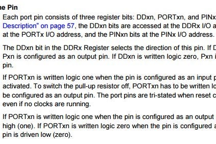
Scrolling down to 10.2.1 Configuring the Pin, you see a mess of abbreviations that is enough to turn off anyone who does not understand what they mean.
Now let’s take a look at the acronyms here so we can understand them better.
First up, DDxn, which refers to DDRB, or the Port B Data Direction Register. Then, PORTxn, which refers to PORTB, or the Port B Data Register. And, PINxn, which refers to PINB, or the Port B Input Pins Address (which we will not address in this Instructable). All of these are shown on page 57 and 58.
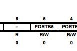
Above is the Data Direction Register for port B.
In the top row, you have the bit numbers. These are basically location designations. Binary is read from right to left, hence the backwards numbering. There are 8 bits in this register, from 0 to 7.
The second row, is the name of the ports in the register. Note that there are two bits that don’t have names. They do not do anything. By the end, these are the names you will use when referencing the various bits in a register.
The third tells you if you can read the bit, write the bit, both, or neither. Bit 6 and 7 do not have a port name, do not do anything, and therefore cannot be written to. All other bits can be read from and written to.
The fourth row tells you what each bit initializes to. In this case, they are all 0s.
There are a total of 6 usable bits, going from 5 to 0, or 0 to 5. Either is acceptable. You may see it referred to like this: DDRB[5,0] or DDRB[0,5].
Shown on the bottom of page 50, it states that a 0 for anyone of these writes the port (and therefore its corresponding pin) as an input. A 1 writes the port as an output. So this is the first thing we want to do in replacing a digitalWrite() command, by replacing the pinMode() command. Before showing you what the actual coding looks like, we will skip to the next register to continue with understanding what to do.
Step 4:
This labels the PortB data Register. This says that each pin within this register is initialized to 0. A 0 writes the port as LOW. A 1 writes the port as HIGH. This is how to replace the digitalWrite() function itself! Shown above is at the top of page 51:
Alright, finally here. Let’s talk about the actual coding now!
First off, we want to “#include <avr/io.h>” so that our commands are understood in the Arduino IDE. As mentioned above, we first need to replace pinMode(). This is done with the DDRB port register. We do this with a “DDRB =” command. For example, let us say you want to write Pin 2 on the ATTiny13A to be an output. So we need look at the datasheet at the diagram again and see that Pin 2 is labelled as PB3. Then we look at the DDRB to see that PB3 is the 4th bit (reading from right to left) in the Register. We need this to be a 1. So we say:
DDRB = 0b00001000;
And that’s it! Pin 2 is set as an output.
Now let us write the pin as HIGH. Again, we know from the figure above from the datasheet that Pin 2 is PB3. Now we need to reference the PORTB Register and find out which bit writes to it. We see it is also the 4th bit (from right to left) in the Register. We need that to be a 1. So we say:
PORTB = 0b00001000;
Pin 2 is now set to HIGH.
Be sure to look at the next Step!
Step 5:
This, though, is not actually how you want to write these commands…
The problem with writing commands like this is that when you do, you are not only writing a 1 to that 4th spot, but you are also writing a 0 to all the other spots as well. If you are writing a program that switches multiple pins on and off at different times, keeping track of how to write the command each time can grow increasingly confusing and can definitely lead to errors!!!
Be happy though, there is a way around this, and it is even easier on the eyes than what we have above. We replace
DDRB = 0b00001000;
with
DDRB |= (1 << PB3);
This is how you will want to write a pinMode() with port manipulation. The “|=” is a bitwise OR assignment. You don’t really need to understand this part. The “1 << PB3” part means that you are going to write a 1 to the PB3 port in the Register, with the << specifically meaning it will look for the PB3 spot wherever it is while ignoring all other bits in the Register.
The one big thing to know here. You can only write a 1 to a bit in a Register in this fashion such that you can only go from 0 to 1 with the |= operator. This is because the whole process is a shorthand method for a binary math operation based on comparisons for the values in the Register.
So when we apply this logic to the PORTB command, it looks like this:
PORTB |= (1 << PB3);
And again, the same rule above applies here as well. Which then begs the question, “How do I turn a pin back to LOW if I cannot write a zero, or if I can only write a 1?”
This is accomplished with a different operator. PORTB &= ~(1 << PB3);
The “&=” is a bitwise AND assignment and the “~” is a bitwise NOT assignment. This is, again, more binary math stuff happening here. But all you need to know is that using this method will unwrite a 1 in the spot you designate and turn it back into a 0.
Step 6:
Here is an example of a sketch of mine that uses port manipulation.
#include <avr/io.h>
void setup(){
DDRB |= (1 << PB3);			//replaces pinMode(PB3, OUTPUT);
DDRB |= (1 << PB4);  			//replaces pinMode(PB4, OUTPUT);
}
void loop()
{
 delay(random(600000, 900000));
 byte state = random(0, 2);
 switch(state)
  {
   case 0:
   PORTB |= (1 << PB3);			//replaces digitalWrite(PB3, HIGH);
   delay(20);
   PORTB &= ~(1 << PB3);		//replaces digitalWrite(PB3, LOW);
   break;
   case 1:
   PORTB |= (1 << PB4);			//replaces digitalWrite(PB4, HIGH);
   delay(20);
   PORTB &= ~(1 << PB4);		//replaces digitalWrite(PB4, LOW);
   break;
  }
}
Add TipAsk QuestionCommentDownload
Step 7:
One of the benefits to pinMode() and digitalWrite() is that you can use variables inside them so you don’t have to go through your entire code if you want to change one pin for another. We can do this with our port manipulations as well with #define. It effectively labels a port/register reference to a variable. It is used as follows:
The above sketch is now rewritten with definitions.
#include <avr/io.h>
#define LED_PIN PB1
#define BUZZER_PIN PB3

void setup()
{
 DDRB |= (1 << LED_PIN);
 DDRB |= (1 << BUZZER_PIN);
}

void loop()
{
 delay(random(600000, 900000));
 byte state = random(0, 2);
 switch(state)
  {
   case 0:
   PORTB |= (1 << LED_PIN);
   delay(20);
   PORTB &= ~(1 << LED_PIN);
   break;

   case 1:
   PORTB |= (1 << BUZZER_PIN);
   delay(20);
   PORTB &= ~(1 << BUZZER_PIN);
   break;
  }
}
For those who are curious, this sketch goes to a prank toy that plugs into a USB at the back of someone’s computer. At random between 10 and 15 minutes, it either blinks a LED or buzzes a buzzer.
Source: ATTiny Port Manipulation (Part 1): PinMode() and DigitalWrite()
- Why use direct port manipulation instead of digitalWrite?
It is roughly 40 times faster and saves memory on the chip. - Which register controls whether a pin is an input or output?
The Data Direction Register, specifically DDRB for Port B. - How do you set a pin as HIGH using port manipulation?
Use the command PORTB |= (1 << PBx) where x is the bit number. - What operator turns a pin back to LOW without affecting others?
Use the bitwise AND assignment combined with NOT: PORTB &= ~(1 << PBx). - What header file must be included to use these commands?
You must include in your code. - Can variables be used with port manipulation?
Yes, you can use #define to label ports as variables for easier code management. - What does the PINxn register refer to?
It refers to the Port B Input Pins Address, though this tutorial notes it will not be addressed. - How are bits numbered in the data direction register?
Bits are numbered from right to left, ranging from 0 to 7.