Summary of BENEFITS OF MULTILAYER PCB AND APPLICATIONS
Printed Circuit Boards (PCBs) have evolved from simple single or double-layer designs to complex multilayer structures essential for modern devices like smartphones and AI robots. Multilayer PCBs feature multiple laminated copper layers connected by vias, pads, and tracks, allowing maximum circuitry in smaller sizes while reducing noise and stray capacitance common in older boards.
Parts used in the Multilayer PCB Project:
- Copper layers
- Laminated sheets
- Soldering components
- Copper tracks
- Vias (PTH, blind, buried)
- Pads
- Holes
Today Printed Circuit Boards (PCBs) have become the integral part in many devices that we use in our daily lives. From handheld portable electronic devices, to industrial machines and heavy equipment, communication devices and consumer electronics we see everywhere these PCBs. Today’s PCBs are very complex and different shapes and materials based. They are flex and rigid and have variety of components that are wired together to perform a specific requirement. However this is only possible in the case of multilayer PCBs.
In older times the PCBs were only single or double layer and did only serve the purpose of simple computation or automation while today these PCBs are more advanced and multilayer and flex PCB are commonly found in motherboards, smart phones, smart watches, biomedical instruments, crypto currency mining devices, artificial intelligence based robotic circuits and many more. Also the manufacturing methods have improved in recent past enabling the faster production, cutting down production cost and reducing size of PCBs cutting down production cost and reducing size of PCBs, see more at Victory PCB.
What Is A Multilayer PCB?
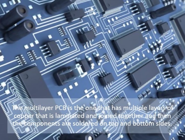
The multilayer PCB is the one that has multiple layers of copper that is laminated and joined together and then the components are soldered on top and bottom sides. The inner layers are actually the double sided circuit that are combined with each other to form one thick PCB with multilayers. The components are electrically connected by means of copper tracks and vias and pads/ holes join the interconnections. The vias are of different types like PTH, blind and buried. The result is the complex PCB with maximum circuitry on smaller PCB size.
Why Multilayer PCB Is Needed?
The advent of complex processing and evolving technology, demands the need of PCB layout procedure that can achieve the desired requirements. Also the problems that were occurring in the single or double sided PCBs like noise and stray capacitance was also an issue that caused the invention of multilayer PCB.
Read more: BENEFITS OF MULTILAYER PCB AND APPLICATIONS
- What is a multilayer PCB?
A multilayer PCB has multiple layers of copper laminated and joined together with components soldered on top and bottom sides. - How are components electrically connected in these PCBs?
Components are connected via copper tracks, vias, and pads that join the interconnections between layers. - Why are multilayer PCBs needed today?
They are required to meet demands of complex processing and to solve issues like noise and stray capacitance found in single or double-sided boards. - Where are multilayer PCBs commonly found?
They are commonly found in motherboards, smart phones, smart watches, biomedical instruments, and artificial intelligence robotic circuits. - What types of vias are used in multilayer PCBs?
The vias include through-hole (PTH), blind, and buried types. - Can multilayer PCBs be flex or rigid?
Yes, modern PCBs can be flex and rigid depending on their specific requirements and materials. - What manufacturing improvements benefit multilayer PCBs?
Improved methods enable faster production, reduced costs, and smaller PCB sizes. - What was the limitation of older PCBs?
Older single or double-layer PCBs could only serve simple computation or automation and suffered from noise and stray capacitance.