Summary of ECEN1400 Final Project- Sensor Spy Ball
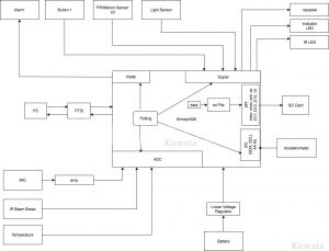
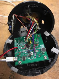
This ECEN1400 final project by a University of Colorado student creates a "Sensor Spy Ball" using an Atmega328p microcontroller to detect environmental changes. The system integrates multiple analog and digital sensors, including accelerometers, PIR detectors, and temperature sensors, to trigger alarms upon detecting significant deviations from initial averages. The hardware features a custom PCB designed in EagleCad with daughter boards for specific components, housed in a 3D-printed enclosure. Although the SD card logging feature was not successfully implemented due to footprint errors, the core sensing and alerting functions were fully operational through software polling logic.
Parts used in the Sensor Spy Ball:
- Atmega328p micro controller
- MPU-6050 Accelerometer
- Panasonic Passive Infrared (PIR) Detectors
- TMP-36 Temperature sensor
- PDV-P8103 Photoresistor
- PMOF-9745 Microphone
- WS2812 Neopixel LED
- SPST momentary Button
- IR333-A IR LED
- PD204-6B IR Photodiode
- PS1420P02CT Piezo
- Breadboard
- EagleCad PCB design files
- FTDI231XS chip
- Labon Hillberry OnShape enclosure model
- PLA and ABS plastic materials
This is the final project for ECEN1400: Introduction to Digital and Analog with Professor Alex Fosidck at University of Colorado at Boulder (Spring 2017). The goal of this project was to make a ball full of sensors which could detect changes in its environment and alert its operator. The ball consists of a custom printed circuit board based on the Atmega328p micro controller interfacing with analog and digital input sensors and output sensors.
List of functional sensors:
- Accelerometer: MPU-6050
- Passive Infrared (PIR) Detectors: Panasonic
- Temperature: TMP-36
- Light: Photoresistor- PDV-P8103
- Microphone: PMOF-9745P
- Neopixel- WS2812
- Button -SPST momentary
- IR LED: IR333-A
- IR Photodiode: PD204-6B
- Piezo: PS1420P02CT
In addition to the above sensors that were fully functional, I failed to implement a micro SD card data logging circuit that utilized a quad buffer to provide level shifting between the 5V Atmega328p and the 3.3V SPI lines of the SD card.
Breadboard
We each developed code for each of the sensors individually so that we could learn about the entire system. After breadboarding the bare minimum circuits we attempted to combine sensing circuits to get an idea of how the polling of the sensors would be required to be written.
Code
The code was developed using Arduino utilizing the following libraries: Wire (for the accelerometer) and the Adafruit Neopixel library. Example code for the accelerometer found here was used as the basis to get raw data from the accelerometer. Logic was created around the accelerometer and gyroscope data to determine if motion was induced on our ball. All other code was created with no additional libraries and purely utilizing analog and digitalReads.
The ball was developed to determine an average of all individual sensor data at initial startup and trigger an alarm if any of the sensors measured a change greater than a threshold. The thresholds of each sensor were determine experimentally by testing the individual sensors in various environments. For the majority of the sensors, if a change was greater than a specified value the alarm would be triggered.
To prevent the sensors from constantly triggering an alarm in the event the environment changes significantly when the ball was first activated, a software re-initialization of the sensor averages was implemented. We felt that this would be useful in the event that the ball is set up in the morning and as the sun sets we would not want the ball to constantly trigger simply from a slow environmental change. This reset was accomplished by iterating a counter value and once a number of iterations of the main loop had been executed the ball would re-initialize the average values for the sensors.
Because the Atmega is unable to read multiple pins simultaneously code was created in such a way to poll the individual pins. We decided to implement a polling method to read sensor data instead of using an interrupt driven system. This was due to the fact that we had too many types of sensors to make use of the three different interrupt routines that could be used to trigger events. With the polling implementation we figured that the sensors would not take longer than 10 ms to read therefore the values would be updated faster than a human could react. We felt that the polling procedure would be adequate in determining human interaction.
Git old and new. Testing: https://drive.google.com/open?id=0B6UPt8IL98yZbFhEcU9LSjhlX3c
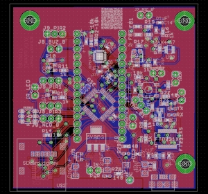
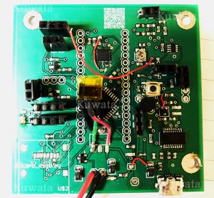
PCB Design
This was my first circuit board board ever and was was created using EagleCad. It was heavily influenced by the arduino nano board layout. This was done for two reasons. One, the nano provides a well known and well experimented with board layout. Two, the nano’s compact size allowed us to use as a backup if the atmega failed to be boot loaded and programed. The header pins in the center of the board was an intentional backup plan to provide us access to the sensors in the event of failure of the micro controller. They were ultimately unnecessary.
Particular care was taken while routing the FTDI signals. It was important to keep traces short, limit number of bends, and create a differential paris for the RX and TX lines. It was also important to match the FTDI231XS capacitors of 47pF exactly to allow for FTDI to be recognized by my computer. I followed the sample schematic found on page 23 of the datasheet: Self Powered Configuration. In addition to this schematic I followed a schematic provided by Professor Fosdick.
The majority of the schematics used to create my circuit board were found in the sample schematics in the data sheets of individual sensors as well as the circuit board schematics provided by Sparkfun. This was very convenient but resulted in an issue here or there that was resolved with PCB re-work with 30 awg wire.
PCB Re-Work
The first issue with the board was the power regulators, 3.3V and 5V as they had the incorrect footprint. I used the footprint of an SOT223 that had the order of the pins different than the part actually in hand. This was corrected by using hook up wire.
I accidentally wired the reset of the FTDI chip a pulled down instead of a pulled up. This resulted in the inability to properly initialize boot loading for the micro controller. I observed that code could be uploaded with a properly timed reset of the Atmega prior to arduino sketch upload. I also noted that I could see the FTDI chip listed in my serial devices connected. I was able to serve my issue by correctly cutting a single trace and pulling up the DTR line. This can be seen in the re-worked board below in the bottom right quadrant of the board. I re-examined my schematic of the FTDI chip and found my mistake.
Additional rework was required for the MPU-6050 to function properly. I initially based my schematic on the a sample schematic available here provided by Sparkfun. After failing to get data out of the accelerometer and checking for an I2C device using the “I2C” Scanner example sketch that the device was not being properly addressed. Re-examining the official data sheet on page 22 Figure 7.2 I was able to identify my issue. The MPU-6050 has the ability to share I2C lines with 2 different addresses: 0x68 and 0x69. The 0x68 is the default for the software library used and is implemented in hardware by setting AD0 (pin 9) to ground. I was able to fix this by wiring the 9th pin to ground. I compared the Sparkfun schematic to the one in the data sheet and found that the V_Logic pin (pin 8) also needs to be held high at 3.3v to establish the logic level for the MPU-6050. Without this the device sets the outputs to be V_Logic which was initially tied to ground through a 10 nF capacitor.
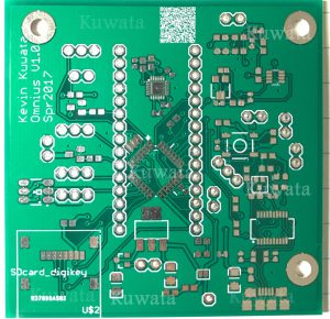
Unfortunately the micro SD card was not fixed in time. The major flaw with the SD card reader was the wrong footprint and pin assignments. I made a custom footprint and flipped horizontally and mirrored the footprint therefore giving totally wrong pins. In addition, I managed to assign the pins 1 position to the left resulting in a unusable footprint. I was able to verify that the SPI lines were correctly turning on the quad buffer giving 3.3v at the correct pads.
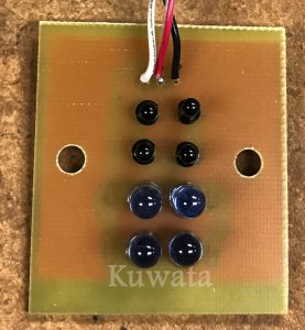
Daughter Boards
Daughter boards for the PIR, photo resistor, button, buzzer, neopixel, and IR emitter/diode were created on one sided copper clad with the toner transfer method. This was an excellent opportunity to learn how to rapidly produce boards to prototype new board layouts without waiting more than a day for feedback on a design.
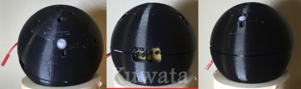
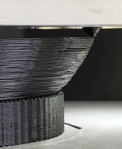
Enclosure
The enclosure of the ball was modeled by Labon Hillberry in OnShape. I 3d printed the enclosure at .6mm layer height in black PLA (instead of PETg) to increase speeds to reduce printing time. The overall printing took over 14 hours on an i3 Hictop FDM printer. Due to the low quality resulting form the 0.6mm layer heights on a 0.8mm nozzle and high speeds, the ball was outsourced to a local company and printed in ABS. If I were to re-do the print I would reduce layer height and not print faster than 50mm/s.
Source: ECEN1400 Final Project- Sensor Spy Ball
- How did the ball prevent constant alarm triggering during slow environmental changes?
A software re-initialization counter was implemented to reset sensor averages after a set number of main loop iterations. - Why was a polling method chosen over an interrupt-driven system?
The team had too many sensor types to utilize the three available interrupt routines on the microcontroller. - What libraries were used to develop the code for the accelerometer?
The Wire library was used along with example code found online to get raw data from the accelerometer. - How was the MPU-6050 address issue resolved on the PCB?
Pin 9 (AD0) was wired to ground to select the default address 0x68, and Pin 8 (V_Logic) was held high at 3.3v. - What caused the failure to implement the micro SD card data logging circuit?
The project used the wrong footprint and pin assignments, resulting in an unusable layout that could not be fixed in time. - Why was the enclosure printed in ABS instead of PLA for the final version?
The initial PLA print had low quality due to high speeds and large layer heights, so it was outsourced to a local company for professional printing. - What tool was used to create the custom circuit board design?
The PCB was created using EagleCad software. - How were the daughter boards for individual sensors manufactured?
Daughter boards were created on one-sided copper clad using the toner transfer method.