Industry Need for Continued Scaling
Technological advances in transistor scaling have had a dramatic effect on consumer electronics and their corresponding use cases. In 1973, Motorola developed the first mobile phone, which weighed 2.5 pounds, was 9 inches long, had limited battery life and only allowed users to make and receive calls. Fast forward to today’s mobile devices that fit in the palm of your hand, with batteries that last all day and more computing power than ever thought possible.
While it has taken 40 years to come this far, innovation has been exceptionally rapid over the course of the past 10 years, and consumer expectations have accelerated at a similar pace. What sort of features and computing capabilities will we expect of our mobile devices five years from now? How about in 10 years? Future improvements largely hinge on the industry’s ability to continue on the path of Moore’s Law by producing ever-smaller transistors with ever-greater performance. Satisfactory scaling fulfills two core requirements: the need for smaller transistors that reduce costs and a parallel need for improved performance and lower power consumption.
To date, transistor scaling has continued in accordance with Moore’s Law down to 32 nm. Engineering challenges, however, are forcing chipmakers to compromise performance and power efficiency in order to reach smaller nodes – unless they switch to new technologies that help better solve these challenges. Today, the semiconductor industry is starting to deploy such new technologies, largely relying on “fully-depleted” transistors for continued scaling and performance gains.
Fully Depleted Silicon Technology
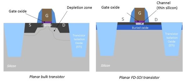
A fully depleted (FD) transistor can be planar or tri-dimensional. In each case, in direct contrast with other technologies commonly used today, the current between source and drain is allowed to flow only through a thin silicon region, defined by the physical parameters of the transistor.
In the planar design of fully depleted technology, transistors are built flat on the silicon. For the three-dimensional alternative, manufacturers fabricate thin vertical “fins” of silicon in which current will flow from source to drain. Additionally, FD transistors can eliminate the need for implanting “dopant” atoms into the channel. These improvements help chipmakers secure gains in both energy efficiency and performance that are required from scaling silicon technology.
For more detail: Fully depleted silicon technology to underlie energy-efficient designs at 28 nm and beyond

