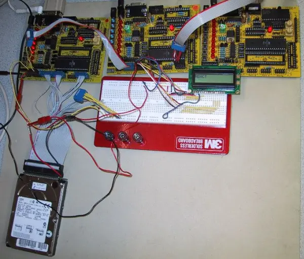
Summary of Hard Drive Based AVR Programmer
This project details the development of a microcontroller programmer utilizing a laptop hard drive to store and transfer ROM files. Originally intended as a WWVB receiver, the team pivoted due to signal issues, opting instead for an IDE hard drive-based system. The design employs two ATMEGA163 microcontrollers in a master-slave configuration to manage user interaction, file retrieval from a FAT32 partition, and in-system programming of an AT90S8515 target MCU.
Parts used in the Microcontroller Programmer:
- ATMEGA163 Microcontroller (Master)
- ATMEGA163 Microcontroller (Slave)
- Laptop Hard Drive (IDE Interface)
- FAT32 Partitioned Storage
- AT90S8515 Target Microcontroller
- LCD Display
- Push Buttons
- Potentiometer
- AC/DC Power Adapter (5V, 1A minimum)
- STK200 Board ISP Header
- CodeVision Compiler Software
The project we are presenting differs from the one initially proposed. Our original plan was to construct a WWVB time-code receiver capable of extracting highly precise time information from a 60 kHz signal provided by the National Institute of Standards and Technology (NIST). However, due to issues with a weak signal and noise interference, we determined that building a time-code receiver would not be viable. As a result, we opted to design a project centered around a laptop hard drive that Richard had in his possession.
Upon studying the capabilities of the hard drive, we decided to create a microcontroller programmer based on its functionality. The primary purpose of this programmer is to enable users to select from various ROM files stored on the hard drive and program the chosen ROM file into a target microcontroller unit (MCU). The design of the programmer incorporates familiar elements of microcontroller-based designs, such as serial communication and the utilization of LCDs as covered in our lectures, alongside new concepts like reading from a FAT32 partitioned hard drive.
High Level Design
Our project aimed to develop an MCU programmer capable of reading ROM data from a standard IDE hard drive. The design of our system involved two ATMEGA163 microcontrollers functioning in a master-slave configuration. The slave MCU was responsible for controlling a FAT32 laptop hard drive, while the master MCU handled user input through push buttons, output via an LCD display, and programming of the target MCU. For the target MCU, we specifically chose the AT90S8515 model due to its advantage of requiring a single instruction for flash programming, unlike the mega163 that requires two instructions. The figure provided below illustrates the interconnections between the major components within our system.
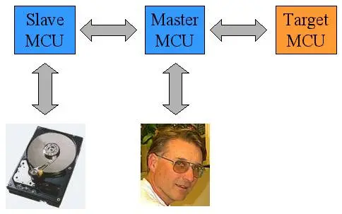
Ideally, we wanted to utilize a single microcontroller, but due to the interface requirements of the hard drive alone, which demanded 24 I/O pins, it was not feasible. In addition, the LCD required a whole port (8 pins), 4 pins were necessary for programming the target MCU, and at least two pins were needed for user input. These I/O requirements exceeded the 36 pins available on a single 8515 or mega163 microcontroller.
To establish communication between the two MCUs, we connected their UARTs together. Upon power-up, the slave MCU performed a hard reset of the hard drive and conducted a listing of the root directory. It stored the essential information about each file, such as the name, file size, and first cluster, in an array in memory. The slave MCU then entered an infinite loop, waiting for a request from the master MCU.
When the master MCU powered up, it sent a request to the slave MCU to obtain a list of all the file names it had found. The master MCU displayed the first file on the LCD and entered a state machine to debounce button presses from the user. The user could cycle through the files, and each file’s information was displayed on the LCD accordingly. Upon pressing the program button, the master MCU sent the index of the currently selected file to the slave MCU. The slave MCU responded to this request through its UART receive complete interrupt. It then read the file from the disk and streamed its contents to the master MCU.
The ROM file format used was the one generated by the CodeVison compiler. An example of this format is illustrated below.
00000D:0000
00000E:94F8
00000F:27EE
000010:BBEC
000011:BFE5
000012:E1F8
000013:BDF1
000014:E1F0
000015:BDF1
In the provided ROM file format, each line consists of a memory address represented by the first six characters, followed by the value to be programmed at that address denoted by the last four characters. Considering that ROM files can be quite large and exceed the available SRAM in a mega163, we implemented a buffering mechanism where only one line is stored at a time. As the data is streamed into the master MCU, each word is converted from ASCII hex values to integers and then programmed into the target MCU’s memory. This programming process occurs in-system, with the master MCU sending commands and data serially to the target MCU’s RESET, MOSI, MISO, and SCK pins.
Hardware Design
For the slave MCU, we established a connection with 24 lines of the hard drive, which proved sufficient for complete control despite the drive providing 40 pins. The majority of these connections were allocated to the 16-bit bi-directional data bus (HD00-HD15) of the drive. By adjusting the direction of the port pins, we successfully enabled both read and write operations without requiring multiplexing or tri-state buffers. The remaining 8 pins corresponded to the 3 address select lines (HA00-HA02), the 2 chip select signals (HCS0-HCS1), reset (HRESET), read (HIOR), and write (HIOW). The signal CSEL was connected to ground to permanently configure the drive as device 0 or master. Additionally, 7 other pins on the hard drive were grounded (pins 2, 19, 22, 24, 26, 30, and 40), while the rest were left unconnected.
An important electrical consideration we encountered was the occurrence of current spikes from the hard drive immediately after power-up. To address this, we utilized an AC/DC power adapter with a minimum sourcing capacity of 1 amp at 5V. Failure to meet this requirement would result in the drive failing to initialize properly.
To establish communication between the slave and master MCUs, the TXD pin of each MCU was connected to the RXD pin of the opposite device.
The LCD was connected to the master MCU and controlled using the LCD libraries provided by CodeVision. We incorporated a potentiometer across Vcc and ground to allow adjustment of the display’s contrast.
Finally, the GND, RESET, MISO, MOSI, and SCK pins available at the ISP header on the STK200 board, which we utilized for programming the target MCU, were connected to output pins of the master MCU.
Program Design
The hard drive operation involves writing to and reading from a set of registers that are accessed through the address select and chip select lines. Data is transferred via the data bus upon receiving a pulse on the read or write line. Instructions are executed by populating the registers with the relevant instruction parameters and then writing the appropriate bit sequence to the command register. The status or alternate status register is polled to monitor the state of the hard drive.
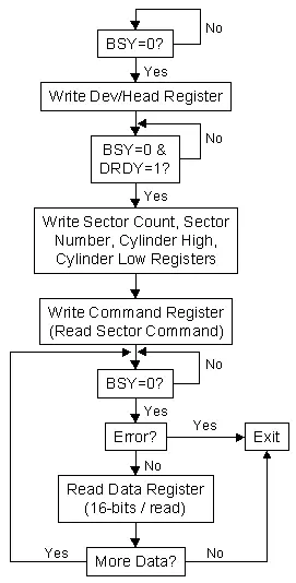
In our project, we specifically implemented the read sector command. This instruction requires a sector address, which can be provided in either LBA (Logical Block Addressing) or CHS (Cylinder, Head, Sector) format. We opted for LBA mode, where sectors are sequentially numbered starting from 0, as it remains consistent regardless of the number of heads per cylinder or sectors per track. Additionally, all sector information stored in the File Allocation Table (FAT) on the disk is also in LBA format. The LBA address, a 28-bit value, is loaded into the device/head, cylinder high, cylinder low, and sector number registers, with the LBA bit set in the device/head register. Since we read only one sector at a time and each sector comprises 512 bytes, we set the sector count to 1, considering the limited 1KB memory of the mega163 microcontroller. The algorithm outlining the interface with the hard drive is depicted in the figure provided. The BSY (Busy), DRDY (Device Ready), and ERR (Error) bits are obtained from the status register.
Upon powering up, the slave MCU initiates a request for sector 0 of the hard drive, which contains the partition records for the drive (in this case, only one partition). This data structure provides the LBA address of the partition’s start, which also corresponds to the location of the boot sector. The boot sector encompasses the BIOS parameter block, which specifies the cluster (where one cluster equals 4KB or 8 sectors in FAT32) for the root directory. To convert the root cluster to a sector address, the following formula is employed (using parameters also found in the BIOS parameter block):
FirstDataSector = ReservedSectorCount + (NumberFATs * FATSize) + BootSector
X_Sector = (X_Cluster – 2) * SectorsPerCluster + FirstDataSector
The root sector contains a sequential list of directory entry structures that provide information about the files within the root directory. The master MCU filters through these files, recording only those with ROM extensions. The key attributes of these files, such as the name, size, and starting cluster (converted to sector address using the above formula), are stored in an array in memory to facilitate servicing requests from the master MCU.
For simplicity, we limited the number of files to eight, as each directory structure occupies 64 bytes, and eight of these structures fill one sector. Additionally, the file size was restricted to 4KB to ensure it does not exceed a cluster’s size, thus avoiding the need for FAT lookups.
During startup, the master MCU requests the files in the root directory from the slave MCU and enters a state machine that handles button presses from the user. The state machine operates with a period of 25ms, which adequately debounces the buttons. As the user presses the cycle button, the master cycles through the file names. When the program button is pressed, the index of the currently selected file is transmitted to the slave MCU. The slave reads the contents of the file from the disk and sends it to the master.
To maintain synchronization during serial communication between the master and slave, we devised a simple request/receive protocol. When the master intends to request a byte from the slave, it first sends a dummy byte and then blocks until the receive complete flag becomes non-zero. On the slave side, when a byte needs to be sent, the MCU blocks until the receive complete flag becomes one (indicating the receipt of the dummy byte), and then proceeds to transmit the byte, thereby unblocking the master. This approach ensures that a byte is not sent unless the master explicitly requests it, signifying its readiness to receive.
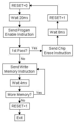
As stated in our high-level design, as each line of the ROM file is received, it is decoded from ASCII to an integer and programmed into the flash memory of the target MCU. The master MCU employs serial downloading, as described in the 8515 datasheet, to program each word in memory. The algorithm for programming the flash memory is depicted in the figure provided.
Results
We achieved a highly satisfying outcome with our project. We successfully programmed an AT90S8515 microcontroller with all the files stored on our hard drive. The MCU functioned seamlessly as if it had been programmed directly from a computer. Furthermore, we utilized CodeVision’s programmer to read the flash contents from the target MCU, and through this verification process, we confirmed that each memory word perfectly matched the specifications outlined in the corresponding ROM file.
Conclusion
Our attempts to develop the WWVB receiver proved to be futile, resulting in a setback of two and a half weeks and incurring a cost of over fifty dollars. In hindsight, we acknowledge the mistake of venturing into unfamiliar territory and straying from mainstream microcontroller design. It was impractical for us to process an ultralow-frequency signal with an amplitude of less than 10uV.
On the other hand, we surprised ourselves by completing the latter design within the given time frame of less than one and a half weeks, despite its relatively complex nature. However, we could have saved hours of debugging had we avoided using the ‘extern’ command. CodeVision, being a non-ANSI C compiler, caused unexpected behavior with ‘extern,’ leading to a loss of two valuable days. Aside from that, along with a few other minor bugs, the project progressed relatively smoothly. Given more time, we would have lifted several restrictions we imposed on the programmer, such as allowing more than 8 ROM files and permitting each file to exceed 4K in size. It would have been intriguing to expand the range of supported target MCUs and incorporate support for EEPROM and lock/fuse bits.
- Why did the team change their original project plan?
The original WWVB time-code receiver was abandoned due to weak signals and noise interference making it non-viable. - How many microcontrollers were used in the final design?
Two ATMEGA163 microcontrollers were used in a master-slave configuration. - What specific microcontroller model was chosen for the target device?
The AT90S8515 was selected because it requires only a single instruction for flash programming. - Why was a single microcontroller not sufficient for the entire system?
A single chip lacked enough I/O pins to handle the hard drive interface, LCD, user input, and programming lines simultaneously. - How is communication established between the master and slave microcontrollers?
Communication is achieved by connecting the UART TXD pin of one MCU to the RXD pin of the other. - What power supply specifications were required for the hard drive?
An AC/DC adapter capable of sourcing at least 1 amp at 5 volts was necessary to prevent initialization failure. - Which file format is supported by the programmer?
The system supports ROM files generated by the CodeVison compiler. - What addressing mode was used for reading sectors from the hard drive?
LBA (Logical Block Addressing) mode was used because it remains consistent regardless of cylinder or head configurations. - Why were the number of files restricted to eight?
Eight files were limited because each directory structure occupies 64 bytes, filling exactly one sector. - What caused a delay of two days during the debugging process?
Unexpected behavior with the 'extern' command in the non-ANSI CodeVision compiler led to the delay.