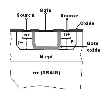
The silicon MOSFET has become a key component in the design of DC/DC converters, providing the high-speed switching and current-handling capability needed to implement high-efficiency, pulse-width-modulation-based control strategies. The drive towards higher efficiency is placing more intense demands on MOSFETs, particularly in designs that have constraints on size, reducing the amount of space that can be given over to heatsinks and other cooling assistance.
The trends are pushing towards the use of MOSFETs that offer reduced Rds(on), as well as offering low switching losses through good charge-storage characteristics. This article will examine a number of the key parameters for MOSFETs in typical DC/DC converter applications.
The metal-oxide semiconductor field-effect transistor (MOSFET) has become a key feature of power-conversion circuits. Its low-charge storage compared to bipolar circuits has made it the component of choice for handling the high-power functions in switched-mode DC/DC converters.
The typical DC/DC converter employs two MOSFETs. One is the control or high-side FET, marked as Q1 in Figure 1. The other is the synchronous or low-side FET, which is marked as Q2 in Figure 1. The name for the low-side FET comes from the fact that the transistor connects the supply rail to ground. The high-side FET, conversely, connects the input and output supply rails.
The high- and low-side FETs are synchronized, which gives the switching converter its commonly used name of synchronous rectifier. Only one switch can be open at any one time and the controller will generally organize switching events to prevent overlap in switching between the two transistors. One transistor will be switched off before the other is allowed to turn on. This behavior prevents losses caused by cross-conduction.
As well as the nominal maximum power that the DC/DC converter can deliver, the two MOSFETs need to handle voltage spikes caused by parasitic inductances and a current level equal to the maximum output current, plus 50 percent of the ripple current. Losses from the two transistors are important. Not only will static losses from the on-resistance through the transistor cause lower efficiency, but so will losses incurred during switching. The switching losses are especially important in DC/DC architectures that employ hard switching; this is where the transistor is exposed to non-zero voltage and current during switching events.
For more detail: MOSFETs Target the Major Efficiency Losses in DC/DC Converters

