
Summary of Music Synthesizer Based on DE0-Nano-SoC
This article details a DIY Music Synthesizer project using a DE0-Nano-SoC board. The system captures audio via a microphone, processes it, and outputs modulated sound through a speaker while displaying the spectrum on an LCD. Users can build this on either a custom PCB or a breadboard, utilizing various analog components like op-amps and capacitors alongside digital converters and FPGA programming in Quartus.
Parts used in the Music Synthesizer:
- DE0-Nano-SoC board
- LT24 LCD Display from Terasic
- Electret microphone
- Two-wire speaker
- Ethernet wire
- PCB or breadboard
- Soldering iron and PCB engraver (optional)
- Battery and USB connector (optional)
- LM386 power amplifier unit
- MCP4821 Digital/Analog Converter
- LT1054 Switched-Capacitor Voltage Converter
- LM317 Adjustable Regulator
- Seven TL081 OPAs (DIP-8)
- One TL082 OPA (DIP-8)
- 2N5432 transistor
- 1N4148 diode
- Various polarized and non-polarized capacitors (ranging from 0.05µF to 4400µF)
- Various resistors (ranging from 18 Ohms to 1MOhm)
Music Synthesizer
This music synthesizer is quite simple : you just have to blow, sing, or even play music in front of the microphone, and the sound will be modulated and sent through the speaker. Its specctrum will also appear on the LCD display.The Music Synthesizer exists in two versions : you may choose to implement it on a PCB, or if you can’t, a simple Breadboard will do.
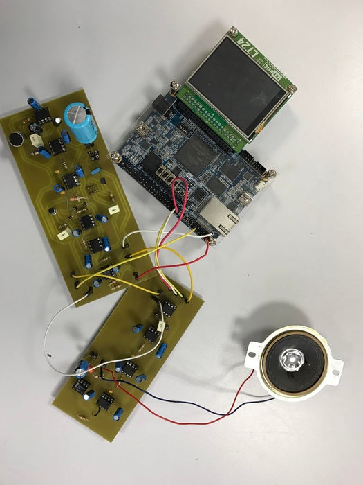
Step 1: Material Needed and Recommendations
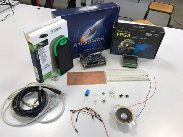
To implement this system, you will need the following :
- a DE0-Nano-SoC board
- a LT24 LCD Display from Terasic
- an electret microphone
- a basic two-wires (ground and supply) speaker
- an Ethernet wire
- a PCB or a breadboard
- a soldering iron and a PCB engraver, if you decide to implement the synthesizer on a PCB
- a battery and its USB connecter (optionnal)
- a LM386 power amplifier unit
- a MCP4821 Digital/Analog Converter
- a LT1054 Switched-Capacitor Voltage Converter
- a LM317 Adjustable Reulator
- 7 TL081 OPAs (DIP-8)
- a TL082 OPA (DIP-8)
- a 2N5432 transistor
- a 1N4148 diode
- 17 10 µF polarised capacitors
- a 1µF capacitor
- 5 100nF capacitors
- a 680nF capacitor
- a 100 µF capacitor
- a 2.2 µF capacitor
- a 1000+µF polarized capacitor (4400 for example)
- a 220 µF polarized capacitor
- a 0.05 µF capacitor
- 4 100 Ohms resistors
- 1 2.2kOhms resistor
- 1 10kOhms resistor
- 1 470 Ohms resistor
- 1 1.8kOhms resitor
- 1 1MOhm resistor
- 1 150 Ohm resistor
- 4 1500 Ohm resistor
Please keep in mind that you may need more components than expected.
We also highly recommend to possess basic knowledge in electronics and SoC design before starting this project.
Step 2: Acquisition Board
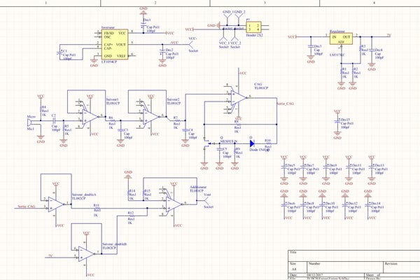
Now that you’ve got everything you need, let’s start by making the acquisition board. The microphone collects nearby sounds, then the signal is filtered by a low-pass filter in order to sample it (and thus respect the Shannon theorem) before it is amplified and is finally recorded by the DE0.
If you are familiar with Altium Design Software and have access to a PCB engraver, you just have to reproduce the schematic shown in the image above, and place the components as we did in the second picture. Otherwise, you may simply recreate this circuit on a breadboard.
In both cases, the values of the resistors, obviously given in Ohms, and the values of the capacitors, given in Farads, are as follows :
- R4 : 2.2k
- R5 : 10k
- R6 and R7 : 100
- R3 : 470
- R1 and R2 : 18 (these resistors are used to adjust the output voltage that should be 2V so these values may be slightly different for you)
- R8 : 1.8k
- R9 : 1M
- R10 : 150
- R11, R12, R14 and R15 : 1.5k
- Dec1 : 2.2µ
- Dec2 : 100µ
- Dec3 : 100n
- Dec4 : 1µ
- Dec5, Dec6, Dec7, Dec8, Dec9, Dec10, Dec11, Dec12, Dec13, Dec14 : 1µ
- Dec15 : +1000µ (4400 for example)
- C1 : 10µ
- C2 : 1µ
- C3 and C4 : 100n
- C5 : 1µ
We’re done with the acquisition board !
Step 3: Audio Output Board
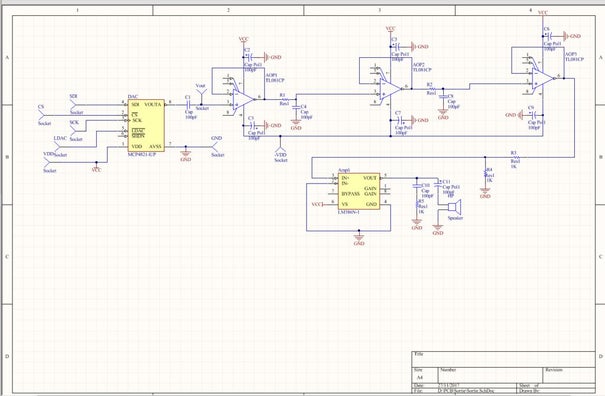
Being able to record sounds is great, but being able to reproduce them is even better! Thus, you’ll need an audio output board, simply consisting of a digital/analog converter, a smoothing filter, a power amplifier and a speaker.
Of course, you can still reproduce the circuit on a PCB (and place the components as shown in the second image) or on a breadboard. In both cases, here are the values for both the capacitors and the resistors :
- R1 and R2 : 100
- R3 and R4 : wires
- R5 : 10
- C1 : 1µ
- C2, C3, C5, C6, C7, C9 : 100µ (polarized)
- C4 and C8 : 100n
- C10 : 0.05µ
- C11 : 250µ
We’re done with the audio output, so let’s move to the software !
Step 4: Quartus Project
To keep things simple, we decided to start from the “my first-hps-fpga” project provided in the CD-ROM included with the DE0-Nano-SoC. All you have to do is open this project and launch “Platform Designer” or “Qsys” from the tools bar, and reproduce the project above. Then, generate the design and compile with Qsys (see the demonstrations for more details).
Step 5: Enjoy !
Now that the HDL files are generated, you just need to launch the Quartus project. Fort that purpose, plug the USB cable into the USB connector (JTAG) of DE0-Nano-Soc. Then, select Tools > Programming on Quartus. Click on Auto Detect, then select the second option. Afterwards, click the FPGA device (the second one), then “Change file” and select the .sof file previously generated. Finally, click “Program/Configure” check board and click “Start” button to launch the file.
Finally, upload the following C code into the DE0 memory. For that purpose, install Putty on a PC (Linux), link the board to it through an Ethernet connection and by plugging the USB cable into the USB connector (UART) of DE0. Launch and configure Putty with a baud rate of 115200, no parity, one bit stop and no flow control settings. Afterwards, force a fixed IPv4 adress to your PC Ethernet port, enter “root” on Putty shell, then “ifconfig eth0 192.168.XXX.XXX” and “password” followed by a password. Open a shell on your PC, go to the project repository, and enter “scp myfirsthpsfpga [email protected]:~/”. Eventually, on the Putty shell, enter “./myfirsthpsfpga”. Enjoy !
Source: Music Synthesizer Based on DE0-Nano-SoC
- How does the synthesizer process sound?
The device captures nearby sounds via a microphone, filters them with a low-pass filter, amplifies the signal, and records it using the DE0 board before modulating and sending it to the speaker. - Can I build this project without a PCB?
Yes, the article states that if you cannot implement it on a PCB, you may simply recreate the circuit on a simple breadboard. - What software is required for the FPGA design?
You must use Quartus Project, specifically launching Platform Designer or Qsys from the tools bar to reproduce the project design. - How do I connect the PC to upload the C code?
You link the board to your PC through an Ethernet connection and by plugging the USB cable into the UART connector of the DE0. - What are the terminal settings for Putty?
You should configure Putty with a baud rate of 115200, no parity, one bit stop, and no flow control settings. - Which specific voltage converter is recommended for this project?
The project requires an LT1054 Switched-Capacitor Voltage Converter. - What is the purpose of the low-pass filter in the acquisition board?
The low-pass filter is used to sample the signal collected by the microphone so that it respects the Shannon theorem. - How do I program the FPGA device after generating the files?
Select Tools > Programming in Quartus, click Auto Detect, select the second option, choose the FPGA device, change the file to the .sof file, and click Program/Configure then Start.
