
Summary of Renesas Electronics Achieves Lowest Embedded SRAM Power of 13.7 nW/Mbit
Renesas Electronics developed a new low-power SRAM circuit using 65nm SOTB technology, achieving a record 13.7 nW/Mbit standby power and 1.8 ns readout speed. This innovation enables maintenance-free IoT devices by eliminating the need for frequent data saving to non-volatile memory during rapid standby-active switching, thereby extending battery life and supporting energy harvesting applications in healthcare and home electronics.
Parts used in the Low-Power SRAM Circuit:
- SRAM prototype
- 65nm node silicon on thin buried oxide (SOTB) process
- Application specific standard products (ASSPs)
- Internal/external non-volatile memory (mentioned as conventional alternative)
Renesas Electronics Corporation announced the successful development of a new low-power SRAM circuit technology that achieves a record ultra-low power consumption of 13.7 nW/Mbit in standby mode. The prototype SRAM also achieves a high-speed readout time of 1.8 ns during active operation. Renesas Electronics applied its 65nm node silicon on thin buried oxide (SOTB) process to develop this record-creating SRAM prototype.
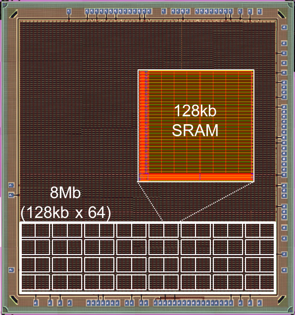
This new low-power SRAM circuit technology can be embedded in application specific standard products (ASSPs) for Internet of Things (IoT), home electronics, and healthcare applications. The fast growth of IoT is requiring all the devices be connected to a wireless network all the time. Hence, products must consume less power to prolong battery life. With this new technology applied, much longer battery life can be achieved enabling maintenance-free applications.
One essential part of the development of IoT applications is the miniaturization of end products. This can be achieved by lowering battery capacity requirement of ASSPs. As an effort to reduce the power consumption in ASSPs for the IoT, there is a technique in which the application is operated in the standby mode and only goes to the active mode when data processing is required.
Now, the conventional way of saving power is to store all important data to an internal/external non-volatile memory and cut off the power supply to the circuit. If the wait time is long enough, this method is effective. But in most of the cases, the device has to switch between standby mode and active mode very quickly causing data-saving and restarting process extremely inefficient. There are even cases where, inversely, this increases power consumption.
In contrary to above, the new technology by Renesas Electronics uses a method where power consumption in standby mode is reduced a lot enabling switching operation to be performed frequently without leading to increased power consumption. Hence, it’s no more required to save data to non-volatile memory. This improves the efficiency further.
The low-power embedded SRAM which is fabricated using the 65 nm SOTB process, achieves both the low standby mode power consumption and increased operating speed. Such features were difficult to achieve with the continuing progress of the semiconductor process miniaturization. Renesas plans to support both energy harvesting operation and development of maintenance free IoT applications that do not require battery replacement by enabling ASSPs that adopt the embedded SRAM with SOTB structure.
Read more: Renesas Electronics Achieves Lowest Embedded SRAM Power of 13.7 nW/Mbit
- What power consumption does the new SRAM achieve?
The prototype achieves a record ultra-low power consumption of 13.7 nW/Mbit in standby mode. - How fast is the readout time during active operation?
The prototype achieves a high-speed readout time of 1.8 ns. - Which process technology was used to develop this SRAM?
Renesas applied its 65nm node silicon on thin buried oxide (SOTB) process. - Can this technology enable maintenance-free IoT applications?
Yes, it allows for much longer battery life enabling maintenance-free applications. - Why is the conventional method of saving power inefficient?
Saving data to non-volatile memory and cutting power is extremely inefficient when devices switch between modes quickly. - Does the new technology require saving data to non-volatile memory?
No, it reduces standby power so frequently switching operations can occur without needing to save data to non-volatile memory. - What types of applications can embed this new SRAM technology?
It can be embedded in ASSPs for Internet of Things, home electronics, and healthcare applications. - How does this technology support energy harvesting?
It enables ASSPs that adopt the embedded SRAM with SOTB structure to support energy harvesting operation.
