Summary of RESEARCHES SOLVE PROBLEMS OF ORGANIC THIN FILM TRANSISTORS BY DEVELOPING NANOSTRUCTURED GATE DIELECTRIC
Amorphous silicon TFTs face mobility limits, leading to OTFT development which suffers from threshold voltage instability. Georgia Tech researchers solved this using a nanostructured gate dielectric. This innovation combines a perfluorinated polymer with a thin metal oxide layer created via Atomic Layer Deposition (ALD) to regulate voltage fluctuations effectively.
Parts used in the Nanostructured Gate Dielectric Project:
- Perfluorinated dielectric polymer
- Thin metal oxide layer
- Atomic Layer Deposition (ALD) technique
Amorphous silicon-based Thin-film transistors (TFTs) are the foundation of many modern-day technologies, such as smartphones and flat-panel TVs. Still, it comes with a few drawbacks like performance limitations due to limited carrier mobility. Provoking the researchers in search of something better.
As a result, Organic thin-film transistors (OTFTs) were developed. OTFTs have solved the problem with carrier mobility to an extent. Although it introduced new problems such as the critical performance parameter of large threshold voltage instabilities. Threshold voltages—also known as gate voltages—are the minimum voltage differential needed between a gate and the source to create a conducting path between the source and drain terminals.
Latest works of the researchers at Georgia Institute of Technology seems to overcome the voltage instability problem with OTFTs. They have developed a nanostructured gate dielectric that can regulate voltage threshold fluctuations in OTFTs.
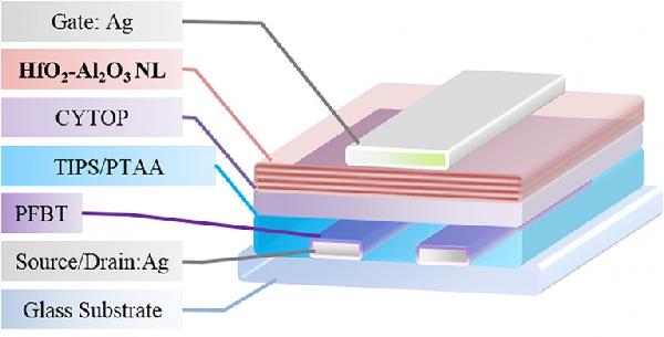
A gate dielectric is an important component of every thin-film transistor. It acts as the electrically insulating layer between the gate terminal and the semiconductor. It should have a high dielectric constant, be very thin, and have a high dielectric strength for the transistor to function at low voltage.
On applying a voltage across the gate electrode, the resulting electric field across this insulating layer changes the density of carriers in the semiconductor layer. It regulates the current that is flowing between the source and the drain electrodes. Many different materials are used to make this insulating layer. Such as dielectric polymers, inorganic oxides or combinations of different organic and inorganic materials.
The Georgia Tech researchers used Atomic Layer Deposition (ALD) technique to build a thin metal oxide layer on top of a perfluorinated dielectric polymer.
Read More: RESEARCHES SOLVE PROBLEMS OF ORGANIC THIN FILM TRANSISTORS BY DEVELOPING NANOSTRUCTURED GATE DIELECTRIC
- What problem do Organic Thin-Film Transistors (OTFTs) have?
They suffer from large threshold voltage instabilities. - How did Georgia Tech researchers solve voltage instability?
They developed a nanostructured gate dielectric to regulate voltage threshold fluctuations. - What is the function of a gate dielectric in a transistor?
It acts as an electrically insulating layer between the gate terminal and the semiconductor. - What materials are commonly used for the insulating layer?
Dielectric polymers, inorganic oxides, or combinations of organic and inorganic materials. - What technique was used to build the thin metal oxide layer?
The Atomic Layer Deposition (ALD) technique was used. - Where is the metal oxide layer placed in this project?
It is built on top of a perfluorinated dielectric polymer. - What happens when voltage is applied across the gate electrode?
The resulting electric field changes the density of carriers in the semiconductor layer. - Why must a gate dielectric be very thin?
A high dielectric constant, very thin layer, and high dielectric strength are needed for low voltage operation.