1 Introduction
1.1 Statement of Purpose
We selected our project because power supplies represent a crucial yet costly element in electrical projects. From an industrial perspective, many product test setups demand multiple precise voltage references, yet the purchased supplies often possess excessive wattage and expense. For hobbyists and students, the price of a single power supply is unreasonably high and escalates proportionally with the requirement for additional outputs. Our emphasis is on the project’s modularity and cost-effectiveness, which are vital factors for both markets.
Objectives
- Goals
• Create a precise tunable power supply with a high level of accuracy (10-20mV).
• Enable vertical stacking of power supply boards without mutual interference.
• Incorporate dual input methods: an analog potentiometer and a digital programmable line.
- Functions
• Deliver adjustable power output with precision between 10 and 20 millivolts.
• Configure input using either an analog, adjustable knob or a digital USB connection.
• Stackable boards feature short protection to prevent malfunction in adjacent boards.
- Benefits
• Inexpensive for expansion, boards can be stacked at a low cost.
• Straightforward setup with clearly defined settings: input/output, CC/CV, analog/digital setpoints.
• Boards can be easily replaced without disruption thanks to short protection, ensuring no risk to other stacked boards or the hub board.
- Features
• A cost-effective modular system that offers low expansion expenses, with boards significantly more affordable than those found in commercial supplies.
• The short protection circuitry guarantees that in the worst-case scenario, only a single header board will malfunction.
• An LCD screen indicator displays all settings, including analog/digital input and CC/CV modes.
2. Design
System Diagram
- System Overview
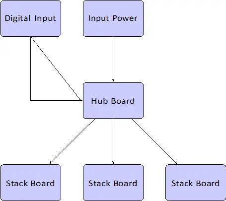
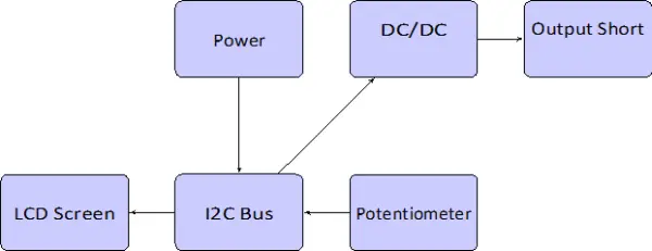
From a technical perspective, the system’s architecture centers on a main card accompanied by attachable subsidiary cards. For consistency in terminology, we identify the main card as the “Hub Board” and the accompanying cards as the “Stack Boards.” The Hub Board is responsible for collecting inputs from various origins and transmitting them to the Stack Boards. Each Stack Board is equipped with its individual board DC/DC converter to configure an output.
- Input Power
The complete system will be powered externally through a banana jack or DC barrel, delivering 12V DC. This power source must have a relatively high wattage capacity since it will need to supply power to all the connected modules in the stack. Therefore, we anticipate a peak requirement of up to 15A.
- Digital Input
One approach to establishing the stack boards’ set points involves utilizing a digital input stream. This process entails operating a computer with a script to access a serial port, through which the computer will receive the quantity of boards from the microcontroller. Subsequently, the computer will request set points for each board before concluding the input request phase. Finally, it will display the confirmed set points alongside their corresponding actual output values.
Hub Board Overview
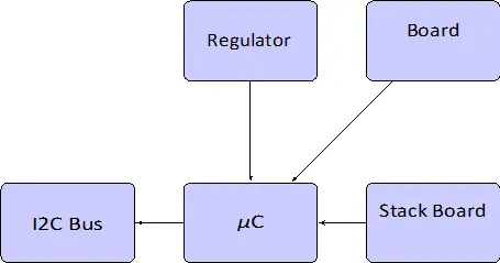
- Regulator
Although the entire board operates on a 12V DC power supply, our microcontroller operates on a 5V DC supply. Therefore, we will employ a linear regulator to decrease the voltage for the microcontroller.
- Microcontroller
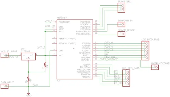
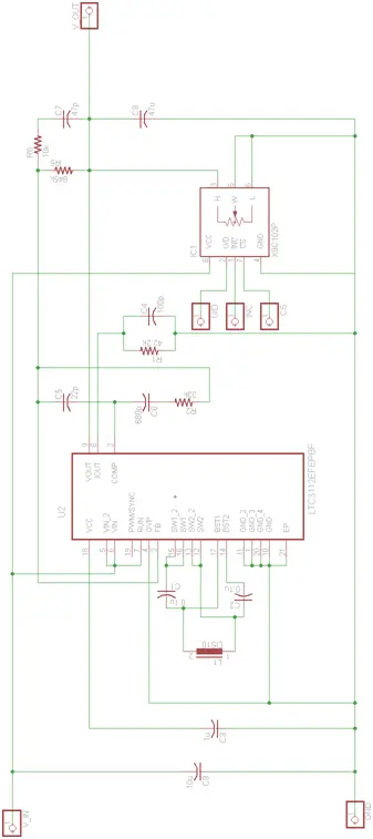
We plan to utilize an AVR ATmega microcontroller in our project, drawing power from the regulator. Its primary tasks include tallying the number of boards and subsequently acquiring potentiometer settings from each stack board. Utilizing this information, it will compute the requisite output values for individual converter chips. This processed data will then be transmitted via an I2C bus to each stack board, along with the essential datastream for the LCD screen. Figure 3 illustrates the configuration of the microcontroller circuit, where inputs originate from the power supply and board sense circuitry, while outputs are directed to both the I2C bus and the LCD screen bus.
- Stack Board Setpoint
The potentiometers will physically reside on the stack boards but will transmit voltages to the hub board. These voltages will then be interpreted by the microcontroller through an ADC. It is crucial to have an ADC with sufficient precision to distinguish between minute voltage variations, around the scale of 10mV.
- I2C Bus
All data computed within the microcontroller, comprising set points, calibration, and LCD screen components, will be transmitted from the microcontroller to an I2C bus for inter-board communication. Employing an 8-pin slave select bus configured for active high, we can utilize the slave select bit for managing all data streams, ensuring communication with a single board at a time.
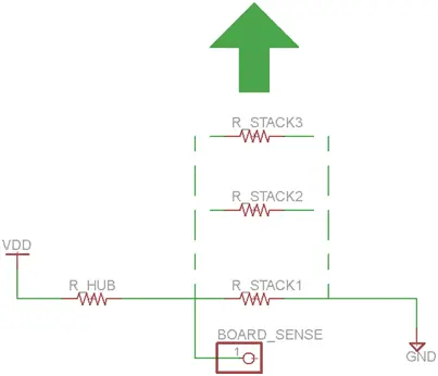
- Board Count Sense
To tally the quantity of boards, our approach involves employing a microcontroller that will interpret a voltage established through a resistive voltage divider. The upper terminal will connect to a consistently fixed resistor on the hub board, while the lower terminal will link to a parallel amalgamation of resistors stemming from the stack boards. Each addition of a stack board will diminish the resistance by a factor equivalent to the number of stack boards. The intermediary value will be directed to the ADC line. Initially, we intended to utilize a 5V supply voltage, but it lacked the adequate range required for the ADC to accurately differentiate. To articulate this in mathematical terms:
VLSB = VDD/210 = 5/1024 ≈ 5mV
Having a least significant bit (LSB) of 5mV, the ADC demonstrates considerable precision across various ranges. This specification outlines the limitations in terms of resistances for our setup.
Rstack/8 Rstack/7 0.005
. Rtop + Rstack/8 Rtop + Rstack/7 . 10
From this information, we have the ability to select the resistor ratio that permits us to detect this slight variation. We opted for resistors within the 10kΩ range to reduce power loss in this circuit section. By setting Rtop at 10kΩ, we systematically varied the resistor ratio to identify the greatest voltage discrepancy.
Voltage Difference between 8 Stack Boards and 1 Stack Board
This sets the optimal ratio at 0.3518. Using that ratio, we can plot the output voltage for each additional board.
Clearly the smallest difference occurs between the 7th and 8th board, which here is 133mV, or 26 LSB’s. This is well within our accuracy range.
- Stack Board Overview
- Power
The daughter boards receive their power input from the 12V DC line transmitted by the hub board.
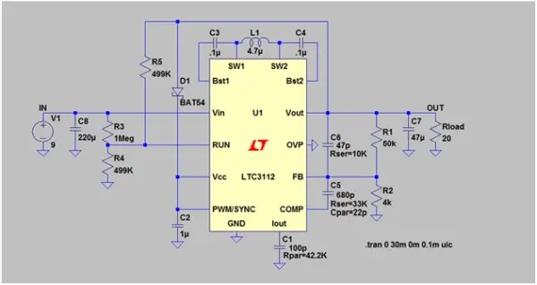
- DC/DC Converter
The central element of the stack board is the converter chip, which functions as a buck/boost switching DC/DC regulator. The current blueprint specifies the utilization of the Linear Technology 3112, capable of generating DC voltages ranging from 3 to 15 volts [2]. The output voltage is determined via a resistor ratio through a typical non-inverting amplifier setup. This ratio is adjusted by employing an I2C-programmable resistor, enabling precise configuration for precise output settings. The formula used to establish the output voltage is as follows:
Vout = 0.8V • 1 + R1
According to the datasheet, it is advised to use resistors in the kilo-ohm range or higher to reduce power wastage. To attain the required voltage range for a stacked board, we sought a precise digital resistor capable of spanning a wide range. Employing a 1024-bit digital resistor [3] and setting R2 at 4kΩ, we adjusted R1 to vary from 0 to 50kΩ. This enables us to calculate the ultimate precision in terms of Least Significant Bits (LSBs):
of LSB’s:
∆Vout
∆Rdig= 15 − 3 = 0.24mV <<< 1 LSB
50k
Although possessing this item is advantageous, another crucial aspect of precision measurement involves determining the voltage output difference between steps, such as setting 782 compared to 783. Given our selection of a linear output, we can calculate this difference in voltage output linearly.
∆Vout = Vout(X + 1) − Vout(X) = 9.8 mV ≤ 1 LSB
Meeting this specification presents a greater challenge, given that achieving precision beyond a 10-bit digital potentiometer seems to be the limit. However, it falls short by just a hair’s breadth of one LSB, so the selected component should suffice for our design.
Figure 6 displays the internal converter designed for stackable modules along with their connected peripherals. The output is configured through a resistor divider, modified using an I2C programmable potentiometer. If necessary, supplementary circuitry can incorporate multiples of 12V to the basic circuit, expanding the potential voltage range of the overall design.
- I2C Bus
Refer to Section 2.2.4
- Potentiometer
The potentiometer must possess high precision and linearity to effectively fulfill its intended function. Additionally, it will be designed as a multi-turn potentiometer to enable users to make more refined adjustments.
- LCD Screen
The LCD screen will exhibit the present configuration points for the board and provide real-time output readings in voltage and current. Additionally, it will feature an indicator to signal the presence of a shorted output on the board, also referred to as the CC/CV mode indicator.
- Output Short Protection
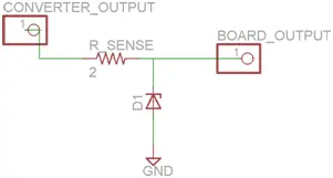
We aim to guarantee the safety of our circuit even in the event of a short or reverse polarity output. To accomplish this, we implement two distinct methods, each addressing a specific scenario. For short circuit protection, we incorporate a sense resistor at the output to prevent excessive current draw. In case of a short, the current surges rapidly, causing a rise in voltage across the sense resistor. By monitoring this voltage, we establish a VOV P threshold that triggers a chip shutdown. The microcontroller measures this level via an ADC pin and initiates the shutdown process if the threshold is surpassed. To safeguard against reverse polarity, we employ a parallel zener diode across the output.
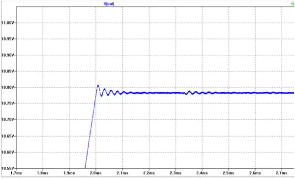
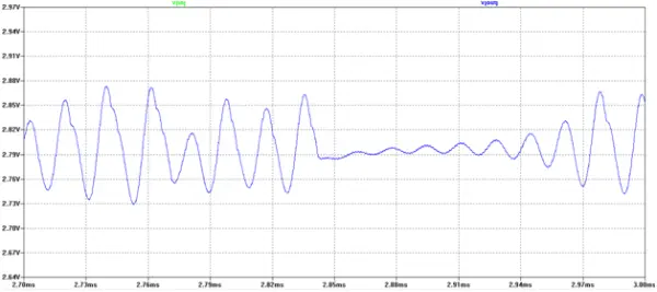
- Simulations
The converter referenced in Table 4 was accompanied by an LTSpice file, allowing us to authenticate our designs [2]. We conducted tests on both ends of the converter, and the resulting plots are displayed below.
Flow Charts
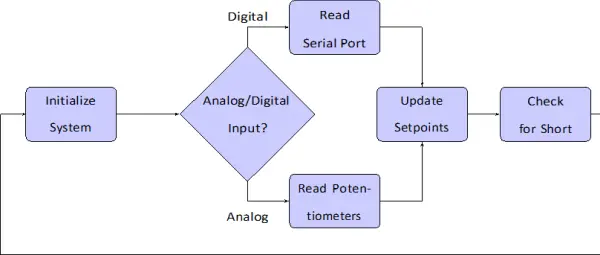
At its most abstract level, this system promptly responds to user input regarding output voltage and maximum output current. Its performance is limited only by the microprocessor’s processing capabilities and clock speed. Upon activation, the system undergoes an initialization phase wherein the hub board assesses the number of connected boards by analyzing the impedance of the output sense line. In non-hub modules, this sense line contains predetermined resistor values, enabling easy identification of other boards by the microprocessor. Subsequently, the system clears the LCD screen to remove any prior displayed values and updates it once the initial setpoints are received. Users then choose between analog or digital input methods to regulate voltage setpoints and current limits, using either potentiometers or serial port data. The internal microprocessor adjusts programmable resistors linked to the relevant thresholds, directly influencing the feedback loop of the DC/DC converter ICs. The system conducts a check for short circuits, promptly shutting down if detected, bolstered by two layers of protection – a fuse and a feedback loop from the controller to the internal converters.
Requirements and Verification
Table 1: Requirements and Verifications
Requirements
LCD
- Check if display powers on
- Check ability to write data to display via serial connection
Verifications
LCD
- Connect display to input voltage and make sure output shows up
- Use the LiquidCrystal library for the Arduino in order to write “Hello World” to display
| Input Power
— Input voltage source should be capable of out- putting 12V +/- 0.5V and at least 15A |
Input Power
— Verify that under stresses of 5A, 10A, and 15A provided by an electronic load, the input source can provide 12V with a 0.5V margin |
| Converters
— Converters must output within 10mV of the output expected by V = 0.8V × 1 + R1 out R2 |
Converters
— Output will be checked against the specified equation for an input of 11.5V, 12V, and 12.5V — Chip will be tested with a breakout board on a breadboard using a standard linear analog po- tentiometer — Output voltage should vary linearly with that resistance, with the output best fit line having a 5% deviation from the mathematical model |
| Analog Potentiometers
— The resistance must change linearly
— Maximum 5% tolerance |
Analog Potentiometers
— Sweep the resistance from minimum to maxi- mum, measuring resistance after each turn; the change in resistance should be under 5% error from a best linear fit line — Compare the maximum resistance of the po- tentiometer with the expected value; ensure that they are within 5% of each other |
| Digital Potentiometers
— Must respond properly to I2C communication
— Linearity of resistance
— Accuracy of resistance between modules |
Digital Potentiometers
— Sweep input bits and observe change in resis- tance using a DMM — Measure resistance at each code, or command word, and plot output; the DNL and INL should be under 1 LSB — Send max resistance code to module, check output resistance. Difference between modules should be under 1% |
Requirements and Verifications, cont.
Requirements Verifications
Microcontroller Microcontroller
- Must be able to transmit I2C data — By using the Arduino program, we will use a
test script to send a ”data counter” script (from 0x00 to 0xFF). We can verify the output us- ing a waveform decoder on the oscilloscope. We can also have another microcontroller read in the datastream. There should be no difference
| — ADC should be accurate to 5mV with up to 1
LSB of error |
— Using a precise voltage reference, sweep the
input reference by 1mV steps. Send the recorded code to the serial output and verify that it changes correctly |
| Linear Regulator
— Output voltage accurate to 5%
Short Circuit Protection — Ability to handle shorts |
Linear Regulator
— Since the output voltage is fixed, test regulator on breadboard and measure accuracy with DMM Short Circuit Protection — While two stackable modules, one with a cir- cuit load and one without, are connected to the hub module, short the stackable module that is not connected to the load. Confirm that the voltage and current ripples are within 50mV and 10mA, respectively. |
Tolerance Analysis
A crucial aspect of our project involves tallying the quantity of stacked modules linked to the hub. To accomplish this, we’ve devised a sensing method employing resistors arranged in parallel, forming a voltage divider circuit that interfaces with our hub board’s microcontroller. Given the microcontroller’s operational range of 0-5V, it’s imperative that our Analog-to-Digital Converter (ADC) exhibits high precision to accurately discern the number of connected boards. However, as more sense resistors are added in parallel, determining the number of boards becomes increasingly challenging due to diminishing changes in overall resistance. With a maximum of 8 boards in mind, the distinction between having 7 or 8 boards equates to roughly 20mV.
Our microcontroller’s ADC is 10-bit, translating to 5mV per Least Significant Bit (LSB). Incorporating a 10% tolerance in the resistors converts our initial 20mV difference to a potential 7mV variance in the worst-case scenario. This transition from a straightforward 4-bit alteration to a significantly more complex 1-2 bit fluctuation poses difficulty in differentiation, resembling noise. Furthermore, environmental factors such as heat, especially pertinent in our high-power, confined system, can influence resistance values, contributing to this variability.
4 Safety
In adherence to the IEEE Code of Ethics, it’s crucial to identify potential hazards for users and take steps to prevent them whenever feasible. Instances where preemptive action or user notification is necessary include instances such as shorting terminals, utilizing an inadequately rated power source for input, and overloading the converter.
To address the first scenario, we’ll employ safety measures against short circuits for each module by integrating a fuse and a zener withstanding load. This setup ensures that component derating and the risk of fire due to excessive current are mitigated. Additionally, informing users about the required specifications for the input power source is essential. Drawing more current than the source can handle may result in blown fuses and improper functioning of converter modules. Furthermore, users need to understand the capabilities of each stackable module. While the voltage range can be adjusted within specific limits for any converter, knowledge of the maximum external circuitry current drawn is crucial before utilizing the module. Otherwise, our current-limiting system implementation might inadvertently cause adverse effects in the external circuitry.