Introduction
The Pyxis camera is an open design for a flexible CCD controller for use in amateur astronomy. The camera was designed in view of the need for a more flexible platform for amateur CCD development. In particular, the controller provides a simple means for interfacing custom hardware (e.g. homemade telescope tracking and slew controllers) directly through a port on the CCD camera controller.
The control card is designed to read two CCDs, an imaging camera and a guiding camera – albeit, not simultaneously. In its current implementation, the imaging camera consists of a Kodak KAF-401/402 (or KAF1602/1603) sensor and the guiding camera uses a Texas Instruments TC211 chip. As of May 2006 Piotr Kucharski successfully modified the Pyxis design to read out the even larger KAF-6303E sensor – this shows that the design is sufficiently flexible to read out most of Kodak’s blue-plus line CCDs. The CCD clock driver and correlated double sampling board is separate from the controller board so that only the clock board needs to be redesigned to support a different CCD sensor. The clock sequences are controlled by a 16 MIPS micro controller (Atmel’s ATMega128) that can easily be reprogrammed to provide custom clock sequences. The camera interfaces to a PC with a low speed USB 2.0 interface (FTDI’s USB245 chip). Custom acquisition software has been written for Windows platform, however the driver code is sufficiently simple to easily modify for other platforms and user specific applications
One of the most attractive features of the Pyxis design is its integrated “smart” power supply. The PC software communicates with the power supply to establish the target CCD temperature for regulation of the temperature on both cameras. A shutter driver for driving Uniblitz (Vincent Associates) 6V solenoid shutter is included on board. The power supply also integrates a simple filter wheel controller that can power a reversible 12 to 24 V DC motor. Means is provided for obtaining relative position feedback from the filter wheel. The power supply can be placed in a low power dissipation mode (turns off the high voltage analog supplies) to conserve battery power. The supply is designed to operate off a 10-14V DC source for efficient field use. All switching supplies have been carefully filtered to ensure very quiet operation. To reduce noise during readout, the high power cooling supplies can be automatically shut down through the PC software.
Performance specifications and features
| Parameter | Value |
| Readout noise (KAF401e sensor)1 | 15 e- RMS |
| Transfer constant | 1.01 e-/ADU |
| Readout time KAF401/402 (KAF1601/1602) | 2 s (8 s) |
| Analog to digital converter resolution | 16 bits |
| Main camera cooling below ambient2 | 40-45 oC |
| Maximum data rate into PC (16 bit data) | 0.5 MHz |
| Communications interface | USB 2.0 |
| Number of independent control lines to CCD board (output only) | 8 |
| Parallel I/O ports | 1 bidirectional, 1 output |
| Filter wheel control | 12-24V DC drive, w. position sensor |
| Shutter control | 6V Uniblitz or other 6V solenoid |
| Input power | 10-14 VDC, 8A maximum draw |
| Power dissipation | Standby: 8.8 WCooling off: 11.5 WCooling on: 41 W |
| CCD output amplifier turn-off during integration | Software selectable |
1. With cooling power supply turned off during readout. Note that cooling can be automatically turned off during readout through the software.
2. Cooling is dependent on thermal load placed on Peltier cooler.
Electrical design
Control board
The heart of the Pyxis camera controller is the ATMega128 which is a 16 MIPS Atmel AVR series micro controller (MCU). This MCU is very easily programmed through an SPI serial interface and Atmel’s inexpensive serial port adapter. A 62 ns instruction time provides sufficient time resolution for generating the CCD clock signals given readout speeds below 500 kHz. All ports and devices share the same 8 bit data bus, except for the main camera port (camera port 1) which uses a dedicated I/O port on the MCU. This was done to ensure efficient data transfer during readout of the CCD (i.e. otherwise, the CCD 1 port would have to be placed in a latched state every time data was sent on the bus either from the ADC or to the USB FIFO). The CCD2 port is intended as the port for the guiding camera (which presumably uses a smaller chip), and therefore does not require as high a readout speed.
The USB interface consists of an FT245BM parallel FIFO device, that is very simple to use, with minimal knowledge of USB transfer protocol required using FTDI’s device drivers. The USB signal ground from the USB cable is connected to Pyxis’s ground through a 50 ohm resistor to eliminate problems with ground loops on battery operated systems.
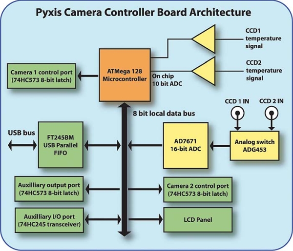
The CCD signals are routed to the single channel, 16 bit, 1.2 MHz sampling ADC through an analog switch and an inverting buffer. The inverting buffer uses a simple ground sensing differential configuration to reduce common-mode noise between the cable ground and signal line. The input video signal range to the controller board is 0 to -10V.
Note that there is no address bus on the system. All control lines to the individual chips use dedicated I/O pins on the MCU. The only multiplexed pins are the SPI programming pins which share two of the I/O pins used for the system data bus. A 16 character by 2 line LCD monitor provides temperature readout, battery voltage status as well as system status messages. The LCD monitor is also tremendously useful when debugging the MCU firmware, allowing the display of variable values and execution points during runtime.
The MCU has an on-chip 10-bit ADC that is used to monitor the temperature of the two CCDs. The controller MCU communicates with the power supply MCU (ATMega16) through a simple bidirectional serial interface in which the controller MCU initiates all transactions.
CCD clock board
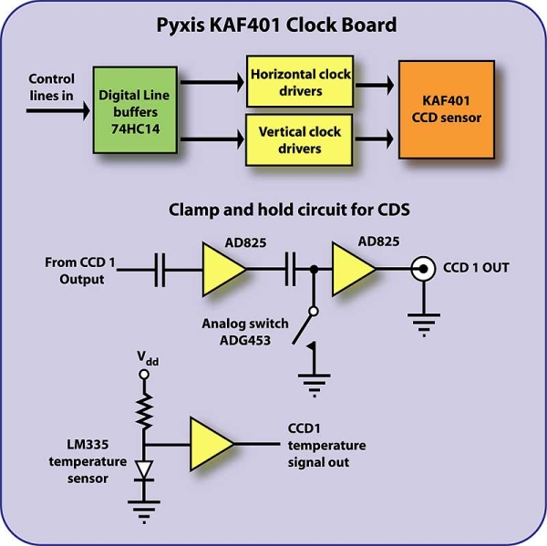
The current CCD clock board is specific to Kodak’s KAF401/402/1602/1603 sensors, although it could be easily modified to support other devices in Kodak’s blue plus line of two-phase sensors. The vertical clock drivers should have sufficient current to operate the KAF1602 sensor with no change in the firmware timings (not tested). The cross over of the horizontal and vertical clock phases can be precisely adjusted by two trim-pots.
Correlated double sampling is performed using a simple clamp and hold scheme similar to that used in the Audine camera. The circuit differs in its use of an ADG453 switch, which has a much lower on resistance than the MAX333 used in Audine. This allows a faster settling time when discharging the clamp capacitor. The ADG453 is also used for one of the clock signals as well as to switch down the voltage appearing on the CCD output amplifier drain. This last feature is necessary to avoid electroluminescence from the output amplifier during long integrations. The CCD temperature is monitored with an LM335 linear centigrade scale temperature sensor. The temperature signal is sent to a calibration preamp before being routed to the controller board.
Cables to the camera head include a 50 ohm BNC coaxial cable for the video signal and an IEEE1284 extension cable for all other signals and power. Only 6′ cables have been tested, however the design should support cables up to 10′ (note that all digital signals are buffered with Schmitt trigger inverters). Three pins are ganged together for each of the Peltier power and return lines to support the required current level. The filter wheel is controlled through a separate cable which consists of two lines for powering the DC motor (reversibly), and a 5V line, signal ground and signal line for the filter wheel position sensor. The position sensor can be electromechanical or use an IR emitter/detector pair for sensing. In the latter case, the 5V line must be replaced by a patch line from one of the unused ATMega128 pins. This is to allow turnoff of the IR emitter during CCD integration (the IR can leak onto the CCD otherwise).
The board has been tested with both the KAF401 and KAF1602ME sensors (November 2005).
Power supply
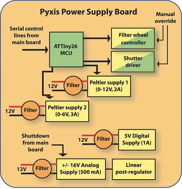
The Pyxis camera distributes most of its power supply regulation to avoid noise coupling on the supply lines going to different boards. The only supply line that is common to all boards is the +5V digital supply; this supply is derived from the 12V input using a linear regulator. The supply outputs ±16V for the analog power using a switching converter with linear post-regulation. These outputs can supply up 500 mA continuously on each output assuming a balanced load. The camera and clock boards each have use low drop-out regulators to obtain the required local analog supplies (±15V or ±12V). The Peltier supplies produce 0-12V @ 2A (Camera 1) and 0-6V @ 3A (Camera 2). The switching signal for the Peltier supplies is derived from the PWM outputs of an ATTiny26 MCU The power supplies for driving the solenoid shutter (up to 24V over voltage opening pulse, 5-9V holding voltage) and the filter wheel motor controller (12-28V adjustable output) use monolithic switching controller chips (LM2586-ADJ). The controller board communicates with the ATTiny26 on the power board to set the Peltier target voltage based on the temperature sensed by the ADC on the ATMega128. The ATTiny26 also deals with operating the filter wheel, using the filter wheel position sensor to determine relative filter wheel position. Each power supply on the board is connected to the 12V input through a common-mode choke to avoid ground-line noise coupling into the analog supplies.
Printed circuit board fabrication: equipment requirements
All the printed circuit boards use surface mount parts. The reason for this is that many of the parts used are only available in SMT packages and the SMT packaging is much more compact and easier to prototype. This last point might not appear obvious until one discovers the ease with which a SMT resistor is interchanged without virtually no damage to the board. Hand fabrication takes little more time than a through hole board. The key is to use very fine gauge low melting point solder and plenty of flux on the solder pads; a flux pen is particularly convenient for applying the flux. An ESD safe temperature controlled iron (e.g. Weller WES51) will prove an invaluable investment; a regular long fine conical iron tip is sufficient for all the work. Also required is an SPI programmer for Atmel’s AVR series MCU ($40). An oscilloscope, preferably a digital sampling oscilloscope with 60 MHz sampling rate or better, will be necessary for troubleshooting and verifying correct CCD clock operation. A PC based sampling oscilloscope suits the job if two computers are available (I use a Link Instruments DSO-2100 USB scope). A multimeter capable of measuring inductance is necessary to fabricate the power supply transformers. It is assumed that anyone building this camera is already proficient in electrical testing and prototyping and has a basic grasp of CCD operation. If you can’t fully understand the operation of the circuit by reading the schematics, then you probably shouldn’t build it! This being said, the boards have been thoroughly tested (three revisions), so things should work on the first try if built correctly.
Software
Firmware
The ATMega128 controller code was written using the CodeVisionAVR C compiler (standard). This compiler provides good high-level language programming support at a modest cost. After spending much time on earlier revisions of Pyxis writing in assembler, I decided that too much time was being wasted debugging apparently innocent, excruciatingly difficult to pinpoint errors. Since much of the code requires 16 bit variables, assembler was simply too clunky for the job. Unfortunately, this means that any modification of the code must be done using CodeVision’s compiler (which isn’t free). However, the existing compiled code can be programmed using Atmel’s free assembler and their SPI programmer. This being said, the source code should be relatively simple to translate to other high level languages because the C code (unlike most assembler code) is quite “readable”.
The main loop updates the LCD display continuously and polls for data on the receive buffer of the USB FIFO chip (the RX# line on the FT245BM). When data is present (sent from the PC to the USB FIFO), the first data byte on the USB receive FIFO is read and execution is redirected according to its value – up to 256 immediate commands can be defined in this way. Once this part of the code is understood, the remaining firmware code is largely self explanatory. Inline assembler is only used to introduce short delays of an exact number of clock cycles.
Device drivers
The drivers are provided in a DLL library (pyxiscom.dll) with a link library compiled for use with Borland C++ Builder 6.0. If you already use C++ Builder, then the library should be simple to link in; just add the “pyxiscom.lib” file to the project and include the header “pyxiscom.h”. The associated DLL (as well as FTD2XX.dll) should sit in your application’s working directory.
If the pyxiscom.lib file must be rebuilt (you are using another language or compiler) you should be aware that pyxiscom links FTDI’s FTD2XX USB driver (FTD2XX.lib, FTD2XX.dll). The FTD2XX.lib version linked must match your own language/compiler (see FTDI’s driver web site for supported compilers).
Acquisition software
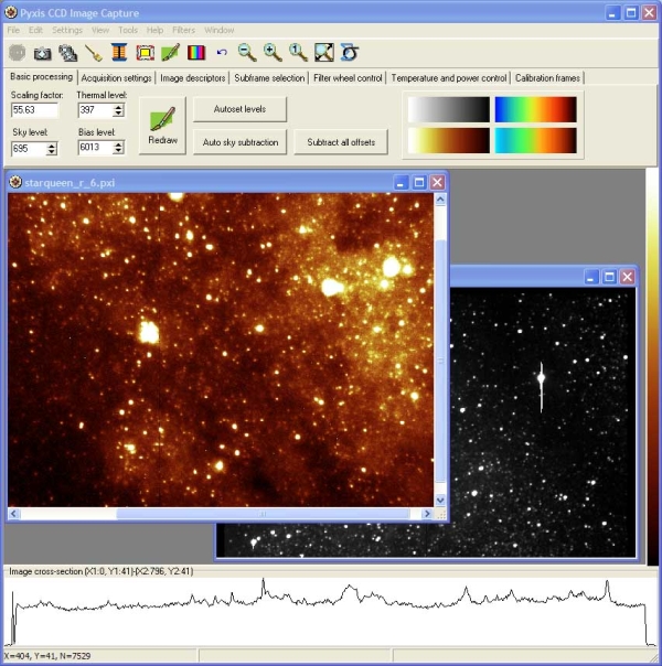
A custom graphical user interface (Pyxis Capture) for Windows has been developed to allow fully integrated operation of the Pyxis camera. This includes a script based control language for situations that may require more user customized control over the acquisition sequences. A basic image processing package is included; images can be composited (up to 5 additive layers, or combined as LRGB), filtered, stacked, background-subtracted and flat fielded. The images can be saved either in Pyxis native format, in FITS format, 16-bit PNG or as 24-bit Windows bit maps.
The Pyxis native image format is useful if most of the image processing is done within Pyxis because it saves the palette model information so that the palette can later be modified. The palettes are based on models derived from bezier curves, so that arbitrary palettes can easily be created. Note that only the models are saved, not the actual 24-bit colour values in the palette. Composite images use the native format exclusively for this very reason; saving only the colour values would not allow the palettes to be edited later.
Several tools are provided for troubleshooting the camera. Tests of the horizontal and vertical clocks can be performed in which the clocks run continuously (this is useful for those who use an analog oscilloscope). A test can be run to ensure that data is being correctly transferred from the controller to the PC. Also, a tool is provided for determining the CCD transfer curve from a series of images. The software improves continuously as my own need for features in my CCD work progresses.
Fabrication cost
A complete bill of materials is provided with an estimate of the part costs in US dollars for August, 2004. The total estimated parts cost, including the KAF401e CCD, is $1600 ($525 is assumed for a grade-1 sensor). This does not include the cost of the instrument case and ancillary hardware, the wiring inside the controller box, the magnet wire to wind the transformers, the shutter as well as any of the hardware associated with the camera housing. It is assumed that people will improvise where these items are concerned. The cost could be easily reduced by over 20% by purchasing larger quantities to fabricate several cameras. In many cases the non-critical parts (e.g. switches and connectors) can be purchased locally at lower cost than through mail-order electronic distributors. Some parts should not be replaced with more inexpensive parts, in particular the large electrolytic capacitors were selected for their exceptionally low ESR. Replacement of these caps will increase the switching power supply noise and may even lead to premature failure of the capacitors (many capacitors cannot sustain the large ripple currents inherent to switching power supplies).
Intellectual property
The information available on these pages is strictly intended for non-commercial use. The provided gerber files should only be used to fabricate small runs of boards resold to cover fabrication costs. An example of a suitable use would be the distribution of a small number of printed circuit boards (PCBs) among members of an amateur astronomy club on a strictly cost-recovery basis (i.e. use for fund-raising within the club is not permitted). A clearly unsuitable use would be the fabrication of any quantity of boards to be resold (even at a marginal profit) over the internet, either as-is or as kits. The compiled firmware/software and associated source code is provided free and may be freely distributed but cannot be modified for use in a commercial product.
Disclaimer
The information provided on these pages is provided as-is with no explicit or implied warranty as to its suitability for any purpose suggested here or otherwise. The author will bear no responsibility for any direct or indirect damages or losses resulting from the use of devices fabricated using the information provided on these pages. The author will bear no responsibility for any direct or indirect damages or losses resulting from the use of software provided on these pages. It is entirely the user’s responsibility to ensure that the fabricated devices meet local electrical code and that the devices are operated in a safe manner. The PC software and MCU firmware is provided as-is and may be freely distributed, used and modified for non-commercial purposes only. The author reserves all copyrights to the software and other documentation linked to these pages. Any use of code derived from the software and firmware must clearly acknowledge the author, Marc R. Baril. Any redistributions of the software and firmware or rebuilds based on the provided source code must be clearly identified as such.
Source: The Pyxis CCD Camera Projects