Summary of Water Cooled Silicon Chips are reality
Georgia Tech researchers developed a monolithic cooling system for 28-nanometer Altera FPGAs by cutting microfluidic passages directly into the chip backsides. This approach places liquid cooling hundreds of microns from transistors, eliminating the need for external heat sinks or fans. The system uses de-ionized water to reduce operating temperatures by over 60 percent compared to air-cooled chips, enhancing performance, longevity, and energy efficiency while enabling denser electronic systems.
Parts used in the Monolithic FPGA Cooling Project:
- Production field-programmable gate array (FPGA) devices
- Microfluidic passages cut into device backsides
- Connection technology for cooling passages
- De-ionized water
- 28-nanometer Altera Corp. FPGA chips
Using microfluidic passages cut directly into the backsides of production field-programmable gate array (FPGA) devices, Georgia Institute of Technology researchers are putting liquid cooling right where it’s needed the most – a few hundred microns away from where the transistors are operating.
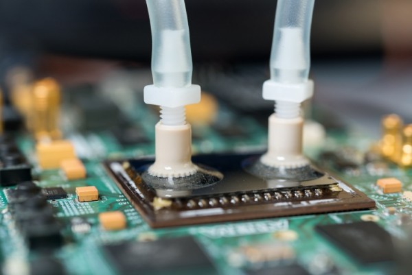
Combined with connection technology that operates through structures in the cooling passages, the new technologies could allow development of denser and more powerful integrated electronic systems that would no longer require heat sinks or cooling fans on top of the integrated circuits. Working with popular 28-nanometer FPGA devices made by Altera Corp., the researchers have demonstrated a monolithically-cooled chip that can operate at temperatures more than 60 percent below those of similar air-cooled chips.
In addition to more processing power, the lower temperatures can mean longer device life and less current leakage. The cooling comes from simple de-ionized water flowing through microfluidic passages that replace the massive air-cooled heat sinks normally placed on the backs of chips.
“We believe we have eliminated one of the major barriers to building high-performance systems that are more compact and energy efficient,” said Muhannad Bakir, an associate professor and ON Semiconductor Junior Professor in the Georgia Tech School of Electrical and Computer Engineering. “We have eliminated the heat sink atop the silicon die by moving liquid cooling just a few hundred microns away from the transistors. We believe that reliably integrating microfluidic cooling directly on the silicon will be a disruptive technology for a new generation of electronics.”
Supported by the Defense Advanced Research Projects Agency (DARPA), the research is believed to be the first example of liquid cooling directly on an operating high-performance CMOS chip. Details of the research were presented on September 28 at the IEEE Custom Integrated Circuits Conference in San Jose, Calif.
For more detail: Water Cooled Silicon Chips are reality
- How does the new cooling technology work?
It uses microfluidic passages cut directly into the backsides of FPGA devices to flow de-ionized water just a few hundred microns from the transistors. - What type of chips were tested in this project?
The researchers worked with popular 28-nanometer FPGA devices made by Altera Corp. - Can this technology eliminate heat sinks?
Yes, the system allows development of systems that no longer require heat sinks or cooling fans on top of the integrated circuits. - Does the cooling improve device lifespan?
Yes, lower temperatures can mean longer device life and less current leakage. - What is the temperature reduction achieved?
The monolithically-cooled chip operates at temperatures more than 60 percent below those of similar air-cooled chips. - Who supported this research effort?
The research was supported by the Defense Advanced Research Projects Agency (DARPA). - Is this the first example of its kind?
Yes, it is believed to be the first example of liquid cooling directly on an operating high-performance CMOS chip. - Where were the research details presented?
Details were presented on September 28 at the IEEE Custom Integrated Circuits Conference in San Jose, Calif.