I. Introduction
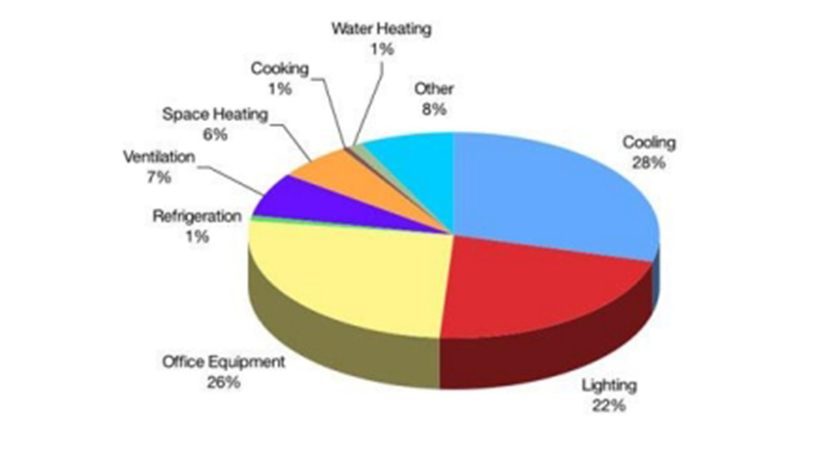
Today, the rising cost of energy and social trend of “going green” has put increasing pressure on commercial property owners to improve the efficiency of their investments. There is good reason for this, too. In the State of California, office buildings represent the single largest user of energy in the commercial sector (Efficiency Partnership). As Figure 1 shows, the majority of the energy consumed by the typical commercial office building is in heating, ventilation, and air conditioning (HVAC), lighting, and office equipment.
Older buildings tend to be less efficient than newer buildings. In HVAC systems, poorly maintained equipment and dated control systems can yield poor energy performance. The energy efficiency of a building can decrease over time due to deferred equipment maintenance, improperly configured controls, user error, and much more. Worse, even modern “green” buildings can suffer from poor efficiency due to the incorrect installation, configuration, and use of increasingly complex building automation and control systems. This project consisted of the design, implementation, construction, testing, and deployment of a wireless sensor network for energy and environmental monitoring in retrofit commercial office installations. The analyzed data generated by this system can be used by building management and owners to identify areas of inefficiency within the building’s major energy using systems – namely heating, ventilation, and air conditioning (HVAC) and lighting.
While suitable for use in new construction, the system was designed for ease-of-use in retrofit installations in existing construction. The final system consists of a self-expanding mesh network of lightweight, battery- and line-powered sensor nodes which are installed at various locations throughout the building to gather power consumption, environmental, occupancy, and space utilization data for a complete energy audit.
2. Requirements
At the beginning of the design process, the following overall design goals and requirements were established for the final system.
- Monitor a variety of standard building automation and control signals to facilitate the
- monitoring of existing building equipment.
- Measure the power consumption of a typical large electrical load within a commercial
- building, such as HVAC, lighting, and office equipment.
- Install a system that will be easy and safe enough for the average non-technical
- individual to perform with limited instruction. As such, as much of the system as
- possible should be wireless and battery-powered.
- Install a system that will not interfere with the normal operation of building equipment
- and controls.
- Provide an easy-to-use interface for the end user to view both real-time and stored data
- from the sensor network.
3. Design
3.1. Platform Selection
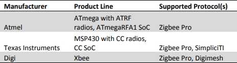
As an embedded systems project, the most fundamental design decision was the selection of a platform for the sensor network. As a wireless sensor networking project, there was the additional constraint that the chosen platform include support for a low-power, lowrate wireless networking protocol. After surveying product offerings from a wide range of embedded device manufacturers, including Atmel, Microchip, Texas Instruments, Freescale,
Silicon Labs, Jennic (now owned by NXP), Digi, and Ember, four platforms were chosen for additional investigation (Table 1).
- Extensive research was then performed on each of these manufacturers’ wireless product
offerings.
Atmel
o Hardware: Atmel manufacturers the ubiquitous AVR line of 8- and 32-bit microcontrollers – most notably the ATmega line. In addition to their microcontroller offerings, Atmel also provides a line of RF transceiver chips – the AT86RFxxx series. The ATMega128RFA1 is Atmel’s current top-of-the-line wireless SoC, and contains the equivalent of an ATmega1281 microcontroller and AT86RF230 2.4GHz wireless transceiver. Atmel also offers the Zigbit line of integrated microcontroller wireless modules.
o Software: Atmel offers a four software wireless networking software stacks for use with their microcontroller and radio hardware.
IEEE 802.15.4 MAC: This IEEE 802.15.4-compliant network stack provides a basic data transport API with support for single-hop star networks. - RF4Control: A Zigbee RF4CE-compliant network stack for use in consumer electronics remote control applications.
Bitcloud: A Zigbee Pro-compliant network stack for use in multi-hop wireless networking applications, including sensor networks, security systems, asset tracking, and more.
Bitcloud Profile Suite: An additional software layer over the Bitcloud stack that provides support for the Zigbee Smart Energy, Home Automation, and Building Automation device profiles.
Development Tools
Development Software: At the time of microcontroller research, AVR Studio 4 was the primary development platform supported for 8-bit AVR development. While this product is somewhat dated when compared to Texas Instruments’ new Eclipse-based Code Composer Studio 4, AVR Studio 4 has a large installed user base and is fairly powerful. However, at the time of this writing, Atmel has released the beta version of their next-generation development environment, AVR Studio 5. This environment is based around Microsoft’s powerful Visual Studio
platform, and is a massive improvement over AVR Studio 4. AVR Studio 5 offers support for both 8- and 32-bit development in the same environment, “Intellisense”-like coding assistance, improved debugging capabilities, and much more.
Development Hardware: At the time of this writing, Atmel’s wireless development hardware options are rather meager; the AVR Dragon and RZ600 platforms are among the few available directly from Atmel.
Several more robust (abeit expensive) platforms are available from thirdparty manufacturers, including Dresden elektronik, MikroElektronika, and Sparkfun. However, Atmel does offer a flexible and wide range of programming and debugging options for all budgets, including the AVRISP mkII, AVR Dragon (used for this project), and JTAGICE mkIII.
Texas Instruments
Hardware:
Texas Instruments offers a full line of 2.4GHz, Zigbee-capable transceivers and system-on-chip ICs. Many of these products are based around the popular MSP430 microprocessor core. Unfortunately, aside from their RF2500 evaluation kit, TI does not offer many economical evaluation or development kits for their wireless offerings; at the time of project research, the cheapest Zigbee-capable wireless development kit was over $500!
Software:
Texas Instruments provides two free wireless networking stacks for use with their wireless hardware: SimpliciTI and ZStack. SimpliciTI is an IEEE 802.15.4-compliant, lightweight wireless stack targeted at smaller, simpler wireless sensor networking applications. SimpliciTI offers a reduced feature set compared to Zigbee. ZStack is a fully Zigbee Pro-compliant networking stack, but will only run TI’s more powerful wireless transceivers and microcontrollers.
Digi
o Hardware: Digi manufactures the XBee line of integrated wireless modules in a convienient through-hole package. These modules are available for the Zigbee or Digimesh protocols. Digimesh is Digi’s own IEEE 802.15.4-compliant lightweight mesh networking protocol. Each XBee module is based around an Ember wireless SoC running custom Digi firmware. This firmware allows the user to configure each XBee as either a “wireless serial cable” or a simple periodicsampling sensor node.
o Software: The end user typically does not modify the code running on the XBee module; rather, the module is configured using Digi’s X-CTU serial configuration utility. This makes setting up a basic network using XBee modules extremely easy. However, this simplified interface also makes XBee modules unsuitable for more complex applications that require the flexibility of running custom code. Given this simple configuration interface, development software is not required for the XBee modules.
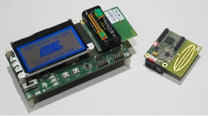
Atmel’s STK500 and STK600 development boards are used in several Cal Poly digital design classes; therefore, the author was already familiar with the AVR Studio 4 development environment. Additionally, the faculty advisor for this project had a significant amount of Atmel wireless development hardware available for use – the RZ200 and RZ201 wireless development kits (Figure 2). Although now discontinued, these kits were still able to provide a decent amount of development hardware for preliminary network testing. Based on extensive research and the aforementioned factors, Atmel’s AVR platform with the Bitcloud networking stack was chosen for this project.
3.2. Zigbee
As a wireless sensor network designed for actual deployment within existing buildings of a variety of construction types and sizes, the ability of the network to grow via multi-hop mesh networking was imperative. Two of the four wireless network stacks offered by Atmel support multi-hop mesh networking: Bitcloud and the Bitcloud Profile Suite. Both of these stacks implement the Zigbee network specification. Therefore, Zigbee was a clear choice when
selecting a wireless networking protocol for this project.
Zigbee, created and maintained by the Zigbee Alliance, outlines a network specification which is based on the IEEE 802.15.4 networking standard. Within the past few years, Zigbee has become widely used for a variety of low-power, low-rate wireless applications, including building automation and control systems, sensor networks, electronic meter reading, and much more. See Figure 3 for a block diagram of a typical Zigbee mesh network. Nodes on a Zigbee network can take on one of three roles: coordinator, router, or end device. All nodes on the network have a “parent-child” relationship (Atmel Corporation).
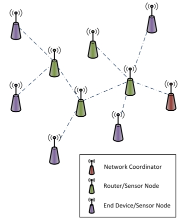
The coordinator forms a Zigbee network. This node holds all configuration and security settings for the network, including the network’s channel, identification number, security key, and security level. Since the network coordinator must have a static address of 0x000, a network can only contain one coordinator at a time. When a network is being created, the coordinator is the first parent node. Given the coordinator’s critical role in the formation of the network, this node cannot enter a sleep state at any time, and is almost always powered from
the wall in an installation.
The router both extends the range of a Zigbee network and acts as a sensor node. Each router holds the same network configuration and security settings as the coordinator, and can act as a parent for new routers and end devices on the network. Additionally, a router can provide all of the functionality of an end device, and perform readings from local sensors.
Given the router’s role in network range extension, router nodes are not allowed to sleep and are typically wall powered.
Zigbee end device nodes are “limited functionality” network nodes. An end device is a “limited functionality” network node, and can only act as a child of the coordinator or a router, and cannot act as a parent to any node. Each end device can only send and receive packets that are buffered by its parent. However, as end devices are allowed to enter a low-power sleep state, these nodes consume very little power and are most often used as batterypowered sensor nodes.
3.3. Bitcloud
As this project will not require support for any of the Zigbee Profiles supported by the Bitcloud Profile Suite, the base Bitcloud network stack was selected. A large portion of Atmel’s current microcontroller wireless offerings, including Bitcloud and Zigbit modules, were originally commercial products produced by a Russian company named Meshnetics. Meshnetics specialized in producing hardware and software for Zigbee mesh network sensor and control networks. The company’s primary evaluation board, the Meshbean, consisted of a Zigbit module coupled with necessary support hardware and several onboard sensors.
In Feburary 2009, Atmel purchased all Meshnetics intellectual property. At this time, the Zigbit module series was re-branded as an Atmel product line, and the Bitcloud network stack was released as a free product for developers using Atmel microcontrollers and wireless transceivers. The Meshbean evaluation board and all other Meshnetics development kits were effectively discontinued.
Unfortunately, this transfer of intellectual property left the documentation and resources for the Bitcloud stack in a state of confusion. While Atmel has added documentation to Bitcloud regarding the deployment of the stack on newer Atmel hardware, there are still many references to the discontinued Meshbean boards in the sample code and documentation. Therefore, a significant portion of this project consisted of reverse-engineering and generating
relevant documentation for Bitcloud.
The Atmel RZ200 and RZ201 evaluation kits shipped with demonstration software running a now defunct Atmel Zigbee stack called Z-Link. Z-Link was discontinued after Atmel’s acquisition of the Meshnetics Bitcloud stack. However, since the RCBs used in these kits have almost identical hardware to Atmel’s current wireless offerings (the Zigbit modules and ATmega128RFA1 SoC), any development work performed on the RCBs is very easy to port to a
more modern platform.
3.4. System-Level Design Overview
After choosing an embedded microcontroller, radio, and network platform, a basic, highlevel system block diagram was developed (Figure 4). Aside from minor modifications, this system architecture was preserved throughout the project.
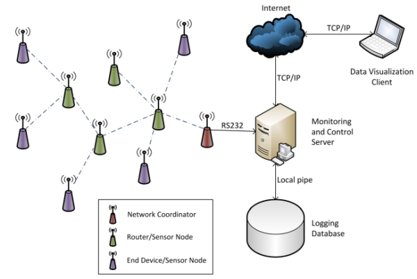
As can be seen in this block diagram, this project encompassed the development of numerous pieces of hardware and software. In this document, these various system components will be broken up as follows:
- Sensor node: This flexible device is the heart of the wireless sensor network, and is
- composed of custom hardware and software. Each sensor node is capable of
- monitoring both external and internal sensors.
- Coordinator: The coordinator acts as a bridge between the wireless sensor network
- and the network management and logging server. The coordinator is based around
- modified Atmel hardware running custom software.
- Network management and logging server: This PC-side application, written in Microsoft
- Visual C#, manages the addition, removal, and logging for all nodes on the network.
- Data collected from the network is written to the SQL database.
- SQL database: Running on Microsoft SQL Server 2008 Express, this database holds the
- settings for all nodes on the network, and all data collected from the network.
- Data visualization application: This PC-side application, also written in Microsoft Visual
- C#, provides an easy-to-use interface for an end-user to view the node data collected in
- any local or remote SQL database.
3.5. Sensor Node Hardware
3.5.1. Overall Design
As the fundamental building block of the network, the sensor node hardware and software design occurred first. In an effort to meet the overall system requirements, the following design goals were outlined for the sensor node hardware:
Non-invasively monitor common building control and automation signals.
Non-invasively monitor power consumption by building loads.
Flexibly support the requirements of a wide variety of installations, including various power sources (battery or wall) and modes of operation (router or end device) with minimal effort on the part of the installer.
- Durability to endure the rigors of installation and use in a commercial environment,
- interfaced with real-world systems.
- Since this wireless sensor network was designed specifically for commercial building
- monitoring applications, one of the major design requirements was that the node hardware
- support interfacing with the signaling standards commonly used in commercial building control
- systems. However,there are a large number of signaling levels and protocols present in
- building control systems; Table 2 presents a sampling of these. To further complicate matters,
- as this project is designed to interface with existing (and likely out-of-date) controls hardware,
- the variety of signals is enormous.
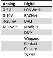
It would be impossible for any lightweight, low power sensor node to support all of these communication standards – each with very specific hardware and software requirements. The original sensor node design addressed this issue with very generic base node hardware that accepted user-installable input cards. The “mainboard” for each node would hold the microcontroller, radio, RF hardware, power supply, and possibly a temperature sensor and realtime clock. The end user of the system would then connect an appropriate input card to the node to add support for the type of signal from the building control system to be monitored. The input card would hold any specialized hardware necessary for interfacing with a given signal, such as analog amplifiers, additional analog-to-digital converters, bus transceivers, and more. This input card-based node architecture would make the system future-proof, as new
input cards could be designed to support newly released communications standards.
Additionally, the end user could easily reconfigure the input capabilities of a system’s nodes during the re deployment of a temporarily installed system. Power is a major concern when designing a wireless sensor node hardware that is to run from a set of batteries for many months, if not several years. Power consumption and battery
lifetime is dependent on a number of factors, including the node sleep/wake patterns, code efficiency, number of external sensors connected, power consumption of the microcontroller and radio, and efficiency of the onboard power supply hardware. All of the Atmel microcontroller and radio offerings are designed to optimally operate from a supply of ~2.7V to ~3.6V – making two series-connected 1.5V AA or AAA cells the perfect power source for the
battery-powered nodes on the network.
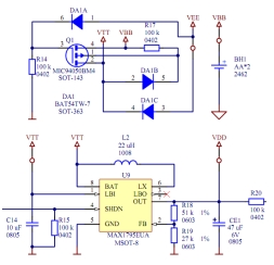
The easiest solution to powering the sensor node from a nominally 3V battery pack (2xAA or 2xAAA) is directly using the battery pack’s output to supply a +3V rail for the sensor node. In fact, Atmel’s own RCB development hardware is powered directly from a battery pack comprised of two series-connected AAA batteries, giving the device a nominal rail voltage of +3V. Over the lifetime of the alkaline cells used in the battery pack, the output voltage of the pack will range from approximately 3.2V with brand-new batteries, to approximately 2.5V with fully discharged batteries.
However, although the Atmel RCBs are directly powered from a 2xAAA battery pack, the Meshnetics Meshbean development boards were designed with a more complex power system. While each Meshbean was also powered by a nominally +3V battery pack, the power rail for each board was supplied by a +3.3V switching boost regulator, as shown in Figure 5 (Atmel Corporation). While the design decisions behind this more complex power system are not known, it is likely that the improved battery life offered by a switching regulator was a major factor.
The Duracell alkaline battery data sheet provides extensive information, shown here in Figure 6 regarding the expected service lifetime of a typical alkaline cell under three types of discharge – constant resistance, constant current and constant power (Proctor and Gamble).
As can be seen, a constant resistance discharge offers the shortest usable cell service life, while a constant power discharge offers the longest usable cell service life. Based on the typical Atmel ATmega datasheet, an AVR microcontroller represents a constant resistance load – as supply voltage increases, the controller’s current draw also increases, and vice versa. A quick survey of the datasheets for several other parts which were considered for use in the final design revealed that many digital chips represent a constant resistance load. Powering a sensor node (a largely resistive load) directly from unregulated alkaline cells would result in the shortest possible service life from the cells.
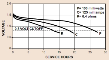
Therefore, several switching regulators were considered for use in the power section of the sensor node hardware design. A switching regulator represents a constant power load – as supply voltage drops, current draw increases, and vice versa. As outlined in the Duracell datasheet, a constant power load is capable of getting the longest possible service life out of an alkaline cell. After significant research, the Texas Instruments TPS61025 3.3V 96% efficient boost regulator was selected. In addition to having a very high efficiency, this part also features a built in low battery monitoring comparator. A node power supply design based around this part could provide a constant +3.3V power rail from any source between 0.9V and 6.5V.
The ATmega128RFA1 is Atmel’s newest offering for wireless microcontroller-based embedded systems. This part combines many of the features and hardware peripherals of the ATmega1281 microcontroller with the AT86RF230 2.4GHz wireless radio in one compact system-on-chip (SoC) package. The ATMega128RFA1 offers the same performance as this discrete microcontroller and radio pair, but with a small board footprint and simplified signal
routing considerations. Therefore, this part was selected as the microcontroller of choice in the original node hardware design.
If each node’s sensor data is time-stamped upon arrival at the network coordinator, timing errors may be introduced to the system based on the latency of the multi-hop network and possibility of data packets being buffered for an extended period of time in installations with poor RF connectivity. Therefore, an I2C real-time clock was incorporated into the original node hardware design to provide each node with the ability to accurately timestamp all sensor data at the point of collection.
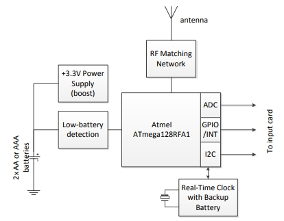
A system-level block diagram of the original conceptual design for the sensor node hardware can be found in Figure 7. Note that all of the major components outlined above are included in this design, including provisions for input cards, the switching regulator, ATmega128RFA1, and real-time clock.
This first sensor node hardware design represented an ideal, best-case architecture. Given the time and resource constraints of this project, however, several aspects of this original design were simplified during the design review process.
While the input card system was a novel solution to providing the sensor nodes with a wide range of user-selectable input capabilities, this architecture would also require significant design work. At the hardware level, input card circuitry would need to be designed for each signaling protocol for which the system might support. This design would require significant research into a wide variety of potentially complex protocols and signaling standards.
Additionally, a connector interface between the node mainboard and input card would need to be design and specified. Such design work could easily add several weeks, if not months, to the project timeline. Therefore, it was decided to design all nodes with the same input circuitry permanently placed on a single sensor node board. This input circuitry would support several of the most common and universal building control signaling standards. Of those listed in Table 2, 0-5V and contact closure were selected as the two signals that would supported on each
sensor node board. The 0-5V voltage interface is commonly used for a wide variety of analog sensors, including pressure, temperature, strain, vibration, and position transducers. The contact closure interface is widely used for monitoring any switching event generated from motion sensors, magnetic reed switches, glass-break detectors, limit switches, thermostatic controls, and more.
One of the fundamental system design requirements was the ability to measure the power consumption of an electrical load. While it would be possible to connect an external amplified current transducer to a sensor node’s 0-5V analog input, the sensor node input collection outlined above would not be able to directly measure current. Therefore, an optional current transformer amplifier was added to the base design. Due to the added cost
and complexity of a node with this amplifier on-board, the amplifier circuitry would only be populated as necessary.
During this design review phase, an on-board temperature sensor was also added to the sensor node hardware design. In particular, it was decided that a digital I2C-interface temperature sensor would be the most appropriate temperature sensor style for this project. Many analog temperature sensors are less accurate and have higher power consumption than their digital counterparts.
While the incorporation of a boost regulator-based power subsystem would have likely resulted in excellent node battery life, this portion of the node hardware design was simplified for a number of reasons. Like many boost regulators available today on the market, the TPS621025 has an excellent efficiency rating at 96%. However, this value only applies to a regulator operating under a medium load – when operated with very light or very heavy loads,
the efficiency of the device suffers greatly. In a typical installation, the sensor node will spend the majority of the time in a very low-power sleep (~500uA max). Therefore, it is very likely that the boost regulator would actually exhibit very poor efficiency when driving a sleeping sensor node.
Due to this uncertainty regarding the actual benefits of a sensor node in powering a wireless sensor node, the boost regulator-based power subsystem was scrapped in favor of a much simpler direct power configuration (similar to that used in the Atmel RCBs). In this new design, the two AAA batteries would directly supply unregulated power to the node’s +3V power rail. A +3.3V voltage regulator would also be included on each node to allow an external
power supply to be used.
Unfortunately, while the Atmel ATmega128RFA1 was in full production at the time of the project design phase, this part was unavailable from any of the major electronics parts distributors, including Mouser, Digi-Key, and Newark. Additionally, even though the ATmega128RFA1 is a highly-integrated SoC with very minimal external component
requirements, the implementation of this chip in the sensor node board design would require the careful selection and layout of several RF components, including a matching network and some kind of printed or chip antennas. Due to these challenges, the ATmega128RFA1 was replaced with an Atmel Zigbit module.
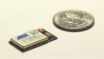
Each Atmel Zigbit module is approximately the size of a postage stamp, and contains an Atmel microcontroller, wireless radio, and necessary RF support circuitry under a metal shield can. Zigbit modules are available with a number of RF configurations, including two onboard chip antennas, an amplified U.FL external antenna connector, an un-amplified U.FL external antenna connector, and balanced, un-amplified RF output. The ATZB-24-A2 Zigbit module chosen for the sensor node hardware design, shown in Figure 8, consists of an Atmel ATmega1281 microcontroller, Atmel AT86RF230 2.4GHz wireless transceiver, and two on-board chip antennas (Atmel Corporation). This module is functionally equivalent to the ATmega128RFA1 SoC, but reduces the amount of RF design work that would need to performed, as the wireless radio and antennas are all located on the module.
Based on preliminary research done on the deployment of Zigbee networks, a simple local configuration and monitoring interface was added to the node hardware design. This interface will allow the system installer to easily configure node settings, such as node mode (router vs. end device) and sleep time in the field without having to re-program the firmware image of the node. In an effort to keep this interface simple and easy-to-use, two LEDs and a
multi-position DIP switch were chosen.
As will be discussed in greater detail in the software development portion of this report, each sensor node requires a unique address on the network. Since the network server will track and store data based on the node address, it is required that each node have a permanent address on the network. Therefore, a 1-wire interface silicon serial number, the Maxim DS2411, was added to the node design. This part holds a unique 48-bit factory laser-engraved
serial number. By basing each node’s address on the serial number stored on this chip, each node can be guaranteed a unique address on the network. Based on the above revisions to the overall sensor node hardware design, the
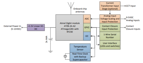
subsystem-level block diagram in Figure 9 was generated.
3.5.2. Analog Input Stage
As outlined in the overall sensor node hardware design, the analog input stage must be able to accurately measure voltages between 0-5VDC. For the sake of a reduced part count and power consumption, the Zigbit module’s on-board analog-to-digital converter will be used to measure the voltage present at the node’s analog inputs. In an attempt to improve the accuracy of this ADC, an external, high-accuracy 2.5V voltage reference will be used as the ADC’s reference. As such, the largest magnitude analog signal that can be accurately measured by the ADC is 2.5V.
Originally, the analog input stage was to be buffered with an operational amplifier (op amp) buffer to both provide input protection for the Zigbit module and reduce the effects of any ADC loading on the accuracy of the resistor divider. The Texas Instruments TLV2450 op amp was selected for its ability to run from a single-sided +3V supply rail, low power consumption, and extremely low-current shutdown mode. However, during the design phase, this buffered design was eliminated due to its increased part count, power consumption, and little effect on the accuracy of the analog input stage.
With a 2.5V reference and input range of 0-5V, the input voltage must be passed through a voltage divider. This voltage division was implemented as a simple resistive divider of two 100kΩ resistors. Additionally, since this input stage will only be used to measure the steady-state DC voltage of the input, a 30Hz low-pass filter was implemented as a 0.1uF capacitor in parallel with the bottom resistor of the divider. This high impedance input stage can be safely connected in parallel across existing equipment without the possibility of harmful loading effects.
Since the sensor node was designed for installation in a commercial environment, likely on industrial equipment, input overvoltage and reverse-polarity protection was built into the analog and contact closure inputs and power supply. At the analog input stage, this input protection takes the form of a fast-acting Schottky clamping diode from the input line to VDD.
During overvoltage events on the input, this diode should “dump” any voltage over VDD onto the node’s positive supply rail. This design was based around material in a Cirrus Logic application note regarding input protection for ADC devices.
3.5.3. Current Transformer Amplifier
One of the major goals of this project was to measure the power consumption of various large electrical loads within a building. In the typical commercial building, HVAC, lighting, and IT/office loads represent the largest energy consumers. Power is defined as the voltage across a given load times the current drawn by that load; therefore, most power measurements require these values.
While HVAC systems range in configuration and power requirements, this project will be designed with the standard electric cooling, gas or electric heat packaged rooftop unit (RTU) in mind. These HVAC units are very common in small- to medium-sized commercial installations, including retail, office, financial, and medical buildings. Depending on the size of the unit and power available at the site, each RTU is usually powered from either a 208V or 480V 3-phase line, and draws between 10-40A. Most commercial building lighting is powered from a singlephase 120V or 277V 20A line, while almost all office and IT equipment loads are run from a single-phase 120V 20A line.
Since this system is designed for easy installation by the end-user without modifications to existing equipment wiring, any “invasive” method of power measurement would be unacceptable. Non-contact forms of AC current measurement are fairly accurate and very commonly used in commercial and industrial load monitoring. Unfortunately, it is very difficult, if not impossible, to implement an accurate non-contact AC voltage measurement system. Therefore, it was decided that all power calculations performed by this network will use the nominal AC line voltage (defined by the system installer) multiplied times the actual, measured AC line current.
One of the most common in-line current measurement techniques is the use of a simple current shunt. A current shunt is a precision, low-resistance load rated for high currents. Based on Ohm’s Law, the known resistance of the shunt, and the measured voltage drop across the shunt, the current through the shunt can be found. However, as an in-line current measurement device, the installation of a current shunt requires cutting power to the load.
Additionally, the shunt offers no isolation between the measurement circuitry and the highvoltage load; in fact, the measurement circuitry is often directly connected the load’s supply!
For these reasons, any in-line current measurement techniques were ruled out for this project. Two of the most predominant non-contact current measurement techniques are the current transformer (CT) and hall-effect sensor. A hall effect-based current transducer measures the magnetic field surrounding a current-carrying wire to determine the current within the line. A current transformer often takes the form of a “clamp” which is placed around a single supply line to the load under measurement. This supply line acts as the primary of the transformer, while the coil within the current transformer is the secondary. Based on the turns ratio of the current transformer, the AC current flowing in the primary line induces a proportional AC current within the secondary coil. By loading the secondary coil with a known “burden” resistance, a measureable AC voltage can be produced.
Since the system is designed for installation on an existing AC line, the current transformer must be of the “split core” variety. A split core current transformer can open for installation around a wire without the need to cut or disconnect the line. The CR Magnetics 3110-3000 current transformer was chosen for this project due to its split core feature, very high current capacity of 75A, and fairly low cost.
Therefore, a current transformer input stage simply needs to be able to accurately measure the magnitude of an AC input voltage between approximately 0-3VAC. Two AC voltage measurement techniques were considered for this stage: an averaging precision fullwave rectifier and an RMS-to-DC IC. An averaging precision full-wave rectifier design would likely consist of several op amps and diodes with an averaging capacitor. Given the 0.7V “on” voltage of the typical silicon diode, the design of such an input stage must be carefully performed to insure good accuracy even at low-voltage inputs. An RMS-to-DC converter IC is a single-chip solution that outputs a DC voltage that is proportional to the root mean square (or statistical mean) of the magnitude of an AC input voltage.
The design of an averaging rectifier for this sensor node would have been fairly challenging, as the node can only provide a +3V, single-sided supply rail. Many designs for such a rectifier require a double-sided supply, and many op amps require supply rails of at least +/- 5V for proper operation. If the design of an averaging precision full-wave rectifier had been attempted, the same Texas Instruments TLV2450 that was selected for the analog input stage voltage buffer would have been used for its low-voltage, single-supply capabilities.
Given the timing constraints of this project, an RMS-to-DC converter IC was chosen as the basis for the current transformer input stage. The Linear Technology LTC1966 was selected as the RMS-to-DC converter as it was the cheapest RMS-to-DC part available on Digikey, at a little over $5 per part in single quantities. Other alternatives on Digikey ranged from $8 to almost $100! Clearly, the RMS-to-DC converter router is not the most economical option; even the “low cost” LTC1966 is likely more expensive than the combined component costs of a discrete averaging precision rectifier. However, the use of an RMS-to-DC converter offers several key design advantages. Since the LTC1966 is rated for operation from a single-sided supply rail between 2.7V and 5.5V, the part can be easily powered from the node’s single 3V positive supply rail (Linear Technology Corporation). Design using this part is very
straightforward – an AC voltage measurement stage can be implemented with just the RMS-toDC IC and a handful of support components. Most importantly, however, the accuracy of the input stage designed around the LTC1966 is almost guaranteed to be very good – especially when measuring dirty or noisy waveforms.
Per the LTC1966 datasheet, the part can only measure AC input waveforms with a maximum differential magnitude of 1V. Therefore, the burden resistance for the current transformer must be chosen such that the transformer’s output when measuring the maximum measurable current is no more than 1V. The schematic of the typical current transformer application circuit is shown in Figure 10.
The CR3110’s datasheet provides the following equations regarding the relationship between measured current, burden resistance, and output voltage.
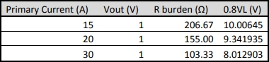
For best linearity R should be chosen such that 0.8VL > V. For the CR3110-3000, Te = 3100 and DCR = 515Ω. Since the sensor node may be used to monitor the current consumption circuits of various sizes, burden resistance values were calculated for maximum currents of 15A, 20A, and 30A. An appropriate burden resistance would be installed on the node based on the circuit to be monitored. Table 3, below, shows the calculated resistances, and clearly indicates that the 0.8VL > V criterion for best linearity is easily met with all of these resistor values.
In addition to LTSpice simulations, a small current transformer prototype was constructed to verify the proper operation of this input stage. This prototype, shown in Figure 11 with the CR3110-3000 current transformer, helped verify that the current transformer input stage would work well in practice. Tests on the prototype board revealed that the current transformer design was sound.
3.5.4. Contact Closure Input
Each contact closure input channel simply consists of an external IRQ GPIO line of the Zigbit module with added overvoltage input protection. The GPIO line’s internal pull-up resistor is used to keep the line in a normally “high” state. A contact closure event between the GPIO line and ground pulls this line low, causing an interrupt on the microcontroller. The input protection scheme on the contact closure inputs is identical to that employed on the analog voltage inputs; a Schottky diode clamps any excessive input voltage to the node’s 3V rail.
3.5.5. Power
With the removal of the switching boost regulator, the design of the power subsystem was quite simple. There are two power connections to the node board – an input for an unregulated, +3V battery pack, and a regulated input for any DC voltage between 5-24V. The LP2950-3.3 voltage regulator was selected for its respectable output current rating of 100mA, low dropout voltage of 40mV, and extremely low quiescent current of 75uA. This regulator was
implemented with a ceramic input capacitor and tantalum output capacitor as required by standard linear voltage regulator design practice and the LP2950 datasheet. A SPDT slide switch between these power sources and the rest of the board controls power to the node. As the final component of the node’s overvoltage input protection scheme, a +3.9V Zener diode was placed between the +3V rail of the node and ground. This diode was to clamp supply rail to
a safe voltage in the event of a transient spike caused by an input overvoltage.
Unless otherwise noted, either a 1uF or 0.1uF bypass capacitor was located on each IC on the node board. Special filtering precautions were taken with the Zigbit module, and both a 10mH inductor and 1uF capacitor were used on the positive supply rail to this part, as outlined in the Zigbit datasheet.
Since the positive supply rail of the node follows the battery pack voltage during battery-based operation. The voltage of the positive supply rail can be measured to determine the current charge state of the battery pack. As previously mentioned, the voltage range of a 2xAAA battery pack can range from approximately 3.2V with brand-new alkaline batteries, to 2.5V with fully discharged batteries. The current voltage of the positive supply rail is measured by the Zigbit module’s ADC_INPUT_0 channel through a ÷3 low-pass voltage divider.
3.5.6. Digital Peripherals
Texas Instruments offers a very large range of analog and digital temperature sensors suitable for a variety of applications. From their product line, the TMP102 and TMP175 I2C Celsius temperature sensors were chosen for further evaluation. The TMP175 has a measurement accuracy of 1.5°C, active current consumption of 100uA, and conversion time of 220mS (Texas Instruments Incorporated). The TMP102 is a much newer and clearly superior part; it has a measurement accuracy of 0.5°C, active current consumption of 15uA, and conversion time of 26mS. However, upon receiving samples of each part, it was discovered that the TMP102’s SOT563 package is incredibly small – 1.7mm x 1.3mm! Since this project is to be hand-soldered, this part was rejected due to its tiny size, and the older, SOIC8-packaged TMP175 was selected.
The final node hardware design calls for the implementation of two digital bus protocols – I2C and 1-wire. Additionally, the local user interface utilizes several GPIO lines to drive LEDs and read from the DIP switch. The I2C bus on each node consists of an I2C master device (the Zigbit module) and two I2C slave devices (the TMP175 temperature sensor and BQ32000 real-time clock). Per standard I2C practice, both the bi-directional serial data (SDA) and serial clock (SCK) lines were pulled up to VDD via 4.7kΩ pull-up resistors.
In addition to the I2C-mandated SDA and SCK lines. The two slave devices also have active-low “alarm” or “alert” lines. On the TMP175, the alert line can be used in conjunction with programmable temperature setpoints to indicate that the sensor’s temperature has passed one of these setpoints. On the BQ32000, the alarm line can be used to indicate when a programmable alarm has fired on the real-time clock. These two alert lines were tied together and to a 4.7kΩ pull-up resistor to VDD, and can be optionally connected to the Zigbit module’s external IRQ7. This gives the option of having alarm/alert events cause an external interrupt in the code.
The 1-wire bus on each node consists of a 1-wire master device (the Zigbit module) and one 1-wire slave device (the DS2411 silicon serial number). This bus was implemented according to the 1-wire standard, with a 4.7kΩ pull-up resistor to VDD.
The local user interface component of the sensor node hardware design consists of two LEDs and a DIP switch. Two surface mount 0603 LEDs – one red, one green – are connected to GPIO lines 0 and 1 through 560Ω current-limiting resistors. A six-position surface mount DIPstyle switch was included to provide an interface for the system installer to configure various node options without having to re-compile the node software. This DIP switch is connected to GPIO lines 2-7 in an active low configuration.
Source: Wireless Sensor Network for Energy and Environmental Monitoring: Helping Old Buildings Go Green