INTRODUCTION
For our final project, we designed a scanning tunneling microscope (STM) that could be used to gather information about the surface topography of metals and semiconductors at the sub-micron scale. The STM is controlled from a graphical user interface running on a PC. The user is able to set various parameters related to the operation of the device such as scan area, sample bias, sample-tip separation and the number of averages per data point (if averaging is turned on). The output of the scanning operation is a data file listing the sample-tip separation at each x-y location. This file can be opened/plotted with various programs (Matlab, Excel etc.) to examine the results. Also, a simple topological image is created on the GUI panel and can be viewed in real-time as the data is taken.

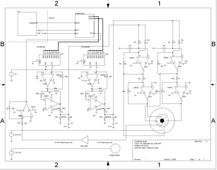
The main motivation behind our project was to interface a microcontroller to a real-time data acquisition system. We also wanted to complete a project that would have an appropriate mix of hardware (analog and digital) and software at both high and low levels. As a result, we decided to construct a simple and cheap scanning tunneling microscope that would be driven by an ATMega163 series microcontroller and operated from a PC.
HIGH LEVEL DESIGN
Ref: A Practical Guide to Scanning Probe Microscopy, TM Microscopes
http://www.tmmicro.com/spmguide/1-1-0.htm
The STM provides information about the surface topology of conductors & semiconductors by measuring the quantum mechanical tunneling current. In order to get the tunneling current, a very sharp tip is scanned over the surface of the conductor/semiconductor being examined. When the scanning tip and the sample surface are brought close together (approximately 1nm apart) and a voltage is applied between the sample and the tip, a finite potential barrier is formed. The height and the width of this barrier can be adjusted by varying the sample-tip separation and the sample-tip voltage. As a result, a finite tunneling current flows between the tip and the sample. This tunneling current approximately has the form:
I = KVe-kd
where K and k are constants depending on the sample-tip voltage and the Fermi energies of the sample and the tip. d represents the sample-tip separation and V stands for the applied bias. Although not exactly accurate, we used this abstraction to calculate the relative heights of individual points on the surface.
The key idea is that the tunneling current varies exponentially with the sample-tip separation, where approximately 1 Angstrom of change in d causes the current to change by an order of magnitude for typical bias voltages and samples. Hence, it is possible to move the scanning tip over the surface and monitor these changes in current in order to calculate the surface topology with sub-micron resolution. This mode of operation is called constant height mode since the height of the tip is held constant. There exists another (more accurate) mode of operation where the current is held constant by using a feedback loop and the tip height is constantly changed to get the desired I value. These changes in the tip height are then recorded and used to calculate the sample-tip separations. This mode of operation is called the constant current mode. In our design, we were able to implement both modes of operation.
The analog circuitry of our design is largely based on the Simple STM design by John Alexander (Introduced and built in AEP130 lab taught by professor Vaclav O. Kostroun). We used a unimorph piezzo disk scanner to move a sharp Iridium-Platinum tip over the sample surface. The control voltages for the scanner are generated by the microcontroller, converted to analog signals by a set of 0808 DACs, inverted to get +/- x/y components, and then amplified or de-amplified to get the user selected step sizes and scan areas. We also implemented various filters to keep the noise amplitude at a maximum of 4 mV so that the tip would remain reasonably stable during operation.
A current-to-voltage pre-amp first amplifies the tunneling current. Then, a comparator is used to subtract a set point voltage corresponding to the sample-tip separation from this signal. The resulting difference is fed into an integrator that keeps the sample-tip separation constant. This difference signal is also amplified and input to the Mega163s ADC to measure the tip-sample separation.
On the software side, the code running on the MCU communicates to the JAVA program running on the PC via the RS232 interface. The MCU interprets a simple command set, performs a calibration, and drives the unimorph scanner according to the specifications transmitted by the PC software. The MCU also takes data (and performs averaging if averaging is turned on by user) and sends it to the PC.
The JAVA code running on the PC gets the user commands from a GUI, notifies the MCU about the users selections and then waits for the calibration to be completed by the MCU. Once that is completed, it starts scanning by issuing a command to the MCU, and receives data points through the RS 232 link (A Serial Port communication program was implemented in JAVA to achieve this). These data points are plotted in real time and a data file listing the results is generated.
The mechanical assembly of our circuit consists of a metal substrate with an adjustable knob that does the coarse positioning of the tip, and a simple assembly for vibration isolation.
For more detail: PC-CONTROLLED SCANNING TUNNELING MICROSCOPE